AI compute demand is rewriting the rules of PCB design. In the past, PCBs served primarily as connection substrates. In the AI era, they are the "backbone" for high-speed signaling and high-power delivery. This shift introduces a new set of challenges that every hardware engineer must address.
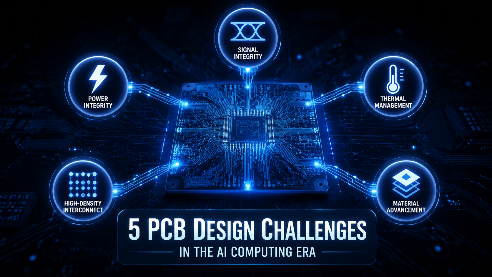
AI server PCBs now typically require 20-30+ layers, with some high-end designs exceeding 70 layers. Below are the 5 core challenges driving this transformation.
The Challenge: With GPU-to-HBM data rates exceeding 112G PAM4 and moving toward PCIe 6.0/7.0, even minor impedance discontinuities or high dissipation factors can cause signal integrity failures. Traditional FR4 substrates are no longer viable.
Design Considerations:
Replace FR4 with low-loss materials like Megtron 6/7, Rogers RO4350B
Implement tight impedance control on all differential pairs
Ensure precise length matching on data buses; avoid T-branch routing
The Challenge: AI chips consume hundreds of watts, with future demands potentially exceeding 100kW per rack. Rapid current swings during compute-to-idle transitions can cause voltage droops and logic errors.
Design Considerations:
Build low-impedance PDNs with dense power/ground planes
Use multi-level decoupling: bulk capacitors for low-frequency, ceramics for mid/high-frequency noise
Implement careful power domain partitioning to avoid noise coupling
The Challenge: AI server rack power demand has risen from 10kW to tens of kW, and is projected to exceed 100kW. High thermal density can cause performance throttling and degrade component reliability.
Design Considerations:
Perform thermal simulation early in the layout phase to identify hot spots
Deploy dense thermal via arrays under GPU/ASIC devices
Consider heavy copper PCBs, metal substrates, or even embedded microfluidic cooling channels
The Challenge: AI accelerators consist of multiple GPU chips in 90×90mm BGA packages, often requiring 512+ high-speed channels. PCB designs are shifting to higher layer counts, denser BGAs, and higher impedance transmission lines.
7-stage HDI designs with 26+ layers are now common. Layer-to-layer registration and material shrinkage control during multiple lamination cycles are critical yield factors.
Design Considerations:
Adopt HDI processes with finer trace/space and microvias
Implement mSAP (modified Semi-Additive Process) for 15-25μm line/space
Use multi-step blind via technology to reduce layer count and board thickness
The Challenge: As 112G evolves toward 224G and 1.6T SerDes, FR4 is being replaced by M7 to M9 ultra-low-loss materials. NVIDIA's Rubin platform uses M8U (Low-Dk2 + HVLP4) with 24-layer HDI for switch trays, while midplane and CX9/CPX designs are moving to M9 (Q-glass + HVLP4), with layer counts reaching up to 104 layers.
Design Considerations:
Plan stackups and process parameters for M7–M9 materials well in advance
Monitor supply trends for T-glass, Q-glass, and HVLP4/5 ultra-low-profile copper foils
AI is redefining the value of the PCB. The board is no longer a passive platform—it is a critical link between compute, memory, and power delivery. For hardware engineers, understanding these 5 challenges is essential to designing products that meet the performance, thermal, and reliability demands of AI workloads.
Ready to tackle these challenges? Contact us to discuss your AI hardware PCBA project.




