In today's fast-paced electronics industry, the demand for efficiency, precision, and speed in product development is paramount. Traditional PCB assembly processes, often manual and prone to error, can bottleneck innovation. How can companies overcome these challenges to bring groundbreaking products to market faster and more reliably? This article delves into the transformative power of Automated Assembly Equipment PCB Solutions, exploring how they are revolutionizing electronics manufacturing and setting new benchmarks for productivity and quality. Zero One Solution Limited, founded in 2011, has swiftly risen to prominence in this very industry, specializing in rapid-response R&D prototype manufacturing and offering one-stop services from PCB design to manufacturing and assembly. We empower clients to accelerate product development and bring innovative solutions to market with exceptional efficiency.
The Evolution of PCB Assembly: From Manual to Automated
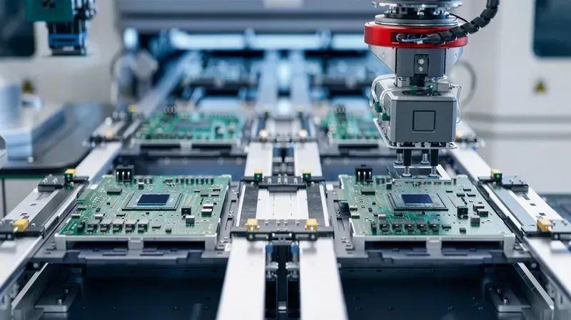
Automated PCB Assembly Line
The journey of Printed Circuit Board (PCB) assembly has seen a profound transformation, moving from labor-intensive manual processes to highly sophisticated automated assembly equipment PCB solutions. This evolution was not merely an incremental improvement but a fundamental shift driven by the relentless demands of modern electronics: increasing complexity, miniaturization, and an insatiable need for higher production volumes and unparalleled precision. Automated solutions directly address the inherent limitations of manual assembly, such as human error, slow throughput, and inconsistency, thereby enabling manufacturers to achieve efficiency levels previously unattainable and solidify their competitive edge in a rapidly accelerating market.
Why was the transition from manual to automated PCB assembly necessary? The manual assembly of PCBs became increasingly inefficient and error-prone as electronic components became smaller and more densely packed, and production demands escalated. Manual processes were also inconsistent, leading to varying quality and higher defect rates. Automation became essential to meet demands for higher precision, faster throughput, and consistent quality.
What were the primary limitations of manual PCB assembly? Manual PCB assembly was plagued by limitations including high rates of human error, slow production speeds, lack of consistency in component placement and soldering, difficulty in handling miniaturized components (e.g., 01005s), and scalability issues that hindered mass production. These factors significantly impacted overall product quality and time-to-market.
How does automation address the challenges of PCB miniaturization? Automated assembly equipment, particularly advanced pick-and-place machines and precision soldering systems, are engineered to handle extremely small and fine-pitch components with accuracy far beyond human capability. Vision systems and robotic precision ensure correct orientation and placement, which is crucial for the reliability and performance of miniaturized PCBs.
What role does demand for higher volumes play in the shift to automated PCB solutions? High-volume production is virtually impossible with manual assembly due to the inherent time constraints and labor costs. Automated assembly equipment PCB solutions offer significantly higher throughput, continuous operation, and scalable production lines, enabling manufacturers to meet aggressive market demands and achieve economies of scale necessary for profitability in consumer electronics and other high-volume industries.
Beyond efficiency, what other benefits did automation bring to PCB assembly? Beyond efficiency, automation brought about substantial improvements in product quality due to reduced defects, enhanced consistency and repeatability across batches, better material utilization with less waste, and improved safety for workers by reducing exposure to hazardous processes. It also enabled faster iterations in R&D and rapid prototyping, crucial for innovation.
Key Components of Modern Automated PCB Assembly Lines
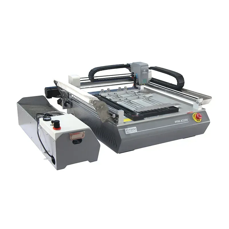
Pick-and-Place Machine and Reflow Oven
A state-of-the-art automated PCB assembly line is a symphony of precision machinery, each component playing a critical role in transforming raw materials into sophisticated electronic circuits. Understanding these key components is fundamental to appreciating the efficiency, quality, and scalability that automated assembly equipment PCB solutions bring to modern electronics manufacturing. From ensuring flawless solder application to meticulously placing miniature components and rigorously inspecting the final product, each system works in concert to deliver unparalleled accuracy and throughput.
Solder Paste Inspection (SPI) Machines SPI machines are crucial for quality control at the very first step of surface mount technology (SMT) assembly. They use 3D imaging to inspect the volume, height, and alignment of solder paste deposits on the PCB pads before components are placed. Defects at this stage, if undetected, can lead to significant rework or scrap later in the process. By ensuring optimal solder paste application, SPI machines drastically reduce common assembly errors such as shorts or open circuits, contributing significantly to overall yield.
Pick-and-Place (PnP) Machines The heart of an automated PCB assembly line, Pick-and-Place machines are robotic devices that precisely pick up surface mount components (SMCs) from feeders and place them onto the PCB. Modern PnP machines boast incredible speed and accuracy, capable of placing tens of thousands of components per hour with micron-level precision, even for miniaturized and fine-pitch components. Their advanced vision systems detect component orientation and position, ensuring correct placement and minimizing errors that would be impossible to achieve manually.
Reflow Ovens After components are placed, the PCB moves into a reflow oven, which is designed to precisely heat the solder paste to its melting point, allowing it to reflow and form robust electrical and mechanical connections between the components and the PCB pads. The oven typically consists of multiple temperature zones (preheat, soak, reflow, and cooling) to ensure a controlled thermal profile. Proper reflow soldering is vital for joint integrity and the long-term reliability of the electronic device. Advanced reflow ovens offer tight temperature control and inert atmosphere options for optimal soldering quality.
Automated Optical Inspection (AOI) Systems AOI systems are post-reflow inspection machines that use high-resolution cameras and sophisticated algorithms to automatically scan the PCB for various defects. These defects can include missing components, incorrect component placement, polarity errors, solder bridges, open circuits, and insufficient solder. AOI provides rapid, consistent, and objective inspection, far surpassing the capabilities of human visual inspection, identifying critical faults before further processing or packaging, thus enhancing overall product quality and reducing manufacturing costs.
Automated X-ray Inspection (AXI) Systems For complex PCBs with hidden solder joints, such as those under Ball Grid Array (BGA) or Quad Flat No-Lead (QFN) packages, Automated X-ray Inspection (AXI) systems are indispensable. AXI uses X-ray technology to inspect solder joints that are not visible to optical systems. It can detect defects like voids, shorts, and misalignments within solder balls and under shielded components. AXI is a critical quality control step, especially for high-reliability applications, ensuring the integrity of connections that are inaccessible through conventional inspection methods.
The integration of these advanced machines into a cohesive automated assembly line empowers manufacturers to achieve unprecedented levels of precision, speed, and consistency. Zero One Solution Limited leverages these cutting-edge technologies to deliver robust and efficient PCB assembly solutions, ensuring the highest quality and accelerated time-to-market for our clients' innovative products.
Benefits of Implementing Automated Assembly Equipment PCB Solutions
Implementing automated assembly equipment PCB solutions offers a transformative impact on electronics manufacturing, fundamentally improving key operational metrics such as precision, speed, and cost-efficiency. This strategic shift from manual processes addresses the escalating demands for miniaturization and complexity in modern PCBs, enabling manufacturers to achieve previously unattainable levels of quality and throughput, directly impacting time-to-market and profitability. Automated systems are engineered to eliminate human error, ensuring consistent component placement and soldering, which is critical for the reliability and performance of advanced electronic devices.
Enhanced Accuracy and Reduced Defect Rates Automated systems, especially those equipped with advanced vision and inspection technologies like AOI and AXI, significantly improve placement accuracy to sub-micron levels, virtually eliminating errors common in manual assembly. This precision leads to a dramatic reduction in defect rates, with some industry reports indicating a decrease of up to 70% in common assembly defects, ensuring higher yield rates and less rework.
Increased Production Speed and Throughput Unlike manual assembly, automated pick-and-place machines can operate continuously at high speeds, placing thousands of components per hour (CPH). For example, high-end pick-and-place machines can achieve speeds exceeding 100,000 CPH, drastically cutting down production cycles. This increased throughput allows manufacturers to meet larger volume demands and accelerate product delivery, crucial in fast-paced markets.
Improved Consistency and Repeatability Automated processes ensure that every PCB is assembled with identical precision and quality, regardless of batch size or operator shifts. This consistency is vital for maintaining product uniformity and meeting stringent quality standards across all units. The repeatability of automated equipment minimizes variations that can occur due to human fatigue or inconsistencies in manual application.
Optimized Material Utilization Automated systems are designed to precisely dispense solder paste and accurately place components, minimizing waste of expensive materials. Through optimized programming and closed-loop feedback, material usage can be reduced by 15-25% compared to manual methods, leading to significant cost savings over time. This efficiency also contributes to a more sustainable manufacturing process.
Reduced Labor Costs and Enhanced Safety While initial investment in automation can be substantial, the long-term reduction in direct labor costs is significant, as fewer personnel are required for repetitive tasks. Furthermore, automating hazardous processes, such as soldering and handling of certain chemicals, greatly enhances workplace safety, reducing risks of injury and associated liabilities. This allows human resources to be reallocated to more complex and value-added activities like supervision and process optimization.
Challenges and Considerations in Automated PCB Assembly
While automated assembly equipment PCB solutions offer transformative benefits, successful implementation requires careful navigation of inherent challenges. These considerations, ranging from significant upfront investment to the necessity of specialized expertise and robust maintenance protocols, are crucial for maximizing efficiency and return on investment. Addressing these hurdles proactively ensures a seamless transition and sustained operational excellence in modern electronics manufacturing.
What are the primary initial investment costs for automated PCB assembly equipment? The primary initial investment costs for automated PCB assembly equipment typically include the acquisition of high-precision machines such as Solder Paste Inspection (SPI), Pick-and-Place (PnP) systems, Reflow Ovens, and Automated Optical Inspection (AOI) units. Additionally, expenses for facility upgrades to accommodate new machinery, software licenses for integrated manufacturing execution systems (MES), and initial training for personnel contribute significantly to the upfront capital expenditure. Depending on the scale and sophistication of the line, these costs can range from hundreds of thousands to several million US dollars, making financial planning a critical first step.
Why is specialized technical expertise essential for automated PCB assembly? Specialized technical expertise is paramount for automated PCB assembly due to the complexity of the equipment and processes involved. Operators and engineers must possess a deep understanding of machine programming, calibration, troubleshooting, and preventive maintenance. This expertise ensures optimal machine performance, minimizes downtime, and maintains the high quality and precision required in PCB manufacturing. Without adequate technical proficiency, the advanced capabilities of automated systems cannot be fully leveraged, potentially leading to inefficiencies and increased operational costs.
What are the maintenance requirements for automated PCB assembly lines? Automated PCB assembly lines demand rigorous and scheduled maintenance to ensure continuous operation and prevent costly breakdowns. This includes routine cleaning of components, lubrication of moving parts, calibration of sensors and nozzles, and timely replacement of wear-and-tear parts. Predictive maintenance strategies, leveraging sensor data and analytics, are also increasingly employed to identify potential failures before they occur. A well-executed maintenance program extends equipment lifespan, maintains output quality, and optimizes overall equipment effectiveness (OEE).
How does Design for Manufacturability (DFM) impact automated PCB assembly? Design for Manufacturability (DFM) is critical for automated PCB assembly as it ensures that the PCB design is optimized for efficient, high-yield production using automated equipment. This involves considerations such as component placement accuracy, pad geometries, solder mask clearances, and board fiducial marks. Adhering to DFM principles minimizes potential assembly errors, reduces rework, accelerates production cycles, and ultimately lowers manufacturing costs. Early DFM integration in the design phase is essential for maximizing the benefits of automation.
What strategies can help overcome the challenges in adopting automated PCB assembly? Overcoming challenges in adopting automated PCB assembly involves a multi-faceted approach. Strategic financial planning, including securing appropriate funding and budgeting for unforeseen expenses, is key for initial investment. Investing in comprehensive training programs for staff is crucial to build internal technical expertise. Implementing robust preventive and predictive maintenance schedules, coupled with readily available spare parts, addresses maintenance needs. Finally, close collaboration between design and manufacturing teams to ensure DFM compliance from the outset is vital for smooth and efficient automated production.
Zero One Solution Limited's Approach to Automated PCB Assembly
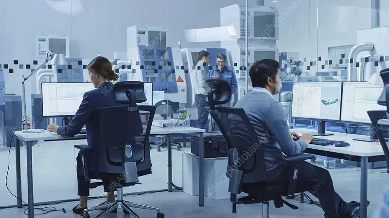
Engineer Working with PCB Prototype
At Zero One Solution Limited, we understand that successful product development hinges on the seamless integration of design, manufacturing, and assembly, especially in the context of automated PCB solutions. Our approach transcends mere component provision, focusing on a holistic, one-stop service model designed to dramatically accelerate your time-to-market and ensure the highest quality output for automated assembly processes. We leverage our deep expertise in rapid prototyping and strategic global presence to deliver unparalleled efficiency and innovation in PCB assembly.
Rapid Prototyping for Accelerated Innovation We specialize in rapid-response R&D prototype manufacturing, providing agile solutions that allow for quick iterations and validation of designs. This significantly reduces development cycles, enabling clients to bring innovative products to market faster and with confidence in their automated assembly compatibility.
Comprehensive One-Stop PCB Service From initial PCB design to manufacturing and final assembly, Zero One Solution Limited offers an end-to-end solution. This integrated approach eliminates the complexities of managing multiple vendors, ensuring consistent quality, streamlined communication, and optimized production for automated assembly equipment PCB solutions.
Strategic Global Presence for Seamless Supply Chain Headquartered in Shenzhen, China, and with a branch office in Dubai, we operate strategically within a robust global PCBA supply chain network. This ensures efficient sourcing of components, access to cutting-edge technologies, and localized support, crucial for optimizing automated assembly operations worldwide.
Expertise in Design for Manufacturability (DFM) Our veteran engineering team possesses extensive knowledge in DFM principles specifically tailored for automated assembly. We collaborate closely with clients during the design phase to optimize layouts, component placement, and material selection, guaranteeing seamless transition to mass production and maximizing automated line efficiency.
Quality Assurance in Automated Environments We implement stringent quality control measures throughout the entire production process, from Solder Paste Inspection (SPI) to Automated Optical Inspection (AOI) and X-ray Inspection (AXI). Our commitment to precision ensures that PCBs produced for automated assembly equipment consistently meet the highest industry standards.
Automated Assembly Equipment PCB Solutions are no longer a luxury but a necessity for companies aiming to thrive in the competitive electronics landscape. By embracing these advanced technologies, manufacturers can achieve unparalleled levels of precision, speed, and cost-effectiveness. Zero One Solution Limited stands as a proven leader in this domain, providing comprehensive, end-to-end solutions from PCB design to manufacturing and assembly. Our strategic global presence, headquartered in Shenzhen and with a branch in Dubai, ensures seamless access to worldwide resources and support, making us the ideal partner for your next project. Ready to elevate your product development and manufacturing capabilities? Contact Zero One Solution Limited today to discuss how our tailored Automated Assembly Equipment PCB Solutions can transform your vision into reality. Let's build the future together!