Introduction: The AI boom is pushing power consumption past 1,000W per chip and driving the shift to Chiplets and high-speed materials. This article explores how these demands are reshaping global PCB manufacturing—from 20oz heavy copper and Any-layer HDI to high-frequency hybrid laminates—and why agile, small-to-medium batch manufacturing is becoming the backbone of global hardware innovation.
Description: Based on AnyPCBA's global manufacturing experience, this article examines the 2026 AI hardware boom—from extreme power density and liquid cooling to Chiplet packaging and high-frequency materials—and explains how agile, advanced PCB manufacturing supports global R&D teams.
If you follow tech headlines in 2026, one trend is undeniable: AI hardware is devouring the world.
From NVIDIA's soaring market value to the rapid rise of domestic AI server manufacturers worldwide, and from massive cloud-based models to the shift toward edge AI PCs and smartphones, the AI wave is sweeping across everything. Compute has become the "new oil" of our era.
But behind the headlines and capital frenzy, a brutal "stress test" is taking place on factory floors. As a manufacturing partner serving global hardware R&D teams, we see a supply chain undergoing a deep structural restructuring. AI's insatiable demand for compute is completely rewriting the rules of PCB manufacturing.
Here is what is happening at the physical layer of the global AI revolution, and what it means for hardware engineers worldwide.
A traditional enterprise server CPU draws roughly 150W to 200W. In the AI era, NVIDIA's latest Blackwell architecture GPUs are pushing power consumption close to 1,000W per chip, with entire server racks exceeding 100kW.
This extreme power density is pushing PCB power delivery to its physical limits:
From "Traces" to "Busbars": To deliver over a thousand amps at sub-1V voltages, copper thickness is shifting from standard 1oz to heavy copper (10oz or even 20oz). On AI server boards, traces are no longer mere traces—they become physical busbars embedded in the board. If etching tolerances are not tightly controlled, these traces can overheat or even melt.
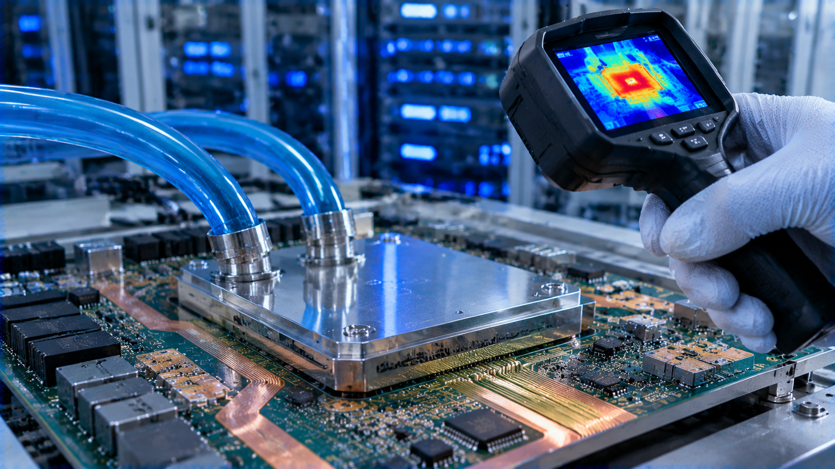
Liquid Cooling and "Deadly Warpage": Air cooling is dead; Direct-to-Chip (D2C) liquid cooling is now standard. This means heavy metal cold plates are bolted directly onto the PCB, applying enormous mechanical stress. If the stack-up is asymmetrical and the PCB warps by even 0.5% under reflow heat or extreme liquid cooling temperature swings, the BGA solder joints beneath the chip will crack, scrapping million-dollar servers.
Moore's Law is slowing. To keep scaling compute power, the industry has pivoted to Chiplet architecture—splitting a large chip into multiple compute dies and packaging them together on a silicon interposer.
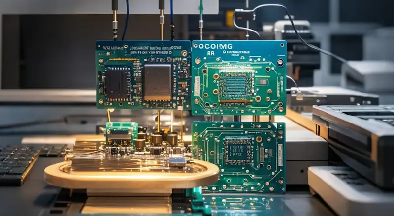
This imposes a massive challenge on PCB manufacturing. Pin density in these advanced packages is surging, with BGA pitch shrinking from 0.8mm to 0.4mm or even smaller. To route thousands of high-speed signals out of the Chiplet package, conventional mechanical drilling is obsolete. The industry is mandating high-order HDI (High-Density Interconnect) and Any-layer HDI, using laser-drilled microvias (smaller than 0.1mm) and mSAP processes to achieve ultra-fine trace widths. This demands extreme layer-to-layer registration precision and advanced alignment equipment.
AI isn't just about density; it's about speed. At 112Gbps or 224Gbps (PAM4), standard FR-4 materials cause catastrophic signal loss.
Global demand for ultra-low-loss materials (M8/M9 grade, PTFE, quartz cloth) far exceeds supply. A handful of Japanese and European manufacturers dominate these high-end material capacities, with lead times stretching to dozens of weeks and prices extremely high.
For global hardware teams, managing signal integrity while using hybrid lamination (FR-4 + high-frequency materials) to balance cost has become a make-or-break challenge.
Against this backdrop, the global electronics supply chain is deeply bifurcated:
On one side, tech giants like NVIDIA and Microsoft have locked up all the high-end capacity from the world's top foundries and leading PCB manufacturers.
On the other side, thousands of small and mid-sized R&D teams worldwide—working on edge AI devices, automotive electronics, and medical instruments—hold the most advanced designs but only need 50 or 500 pieces for prototyping or small-batch trials. They face an awkward dilemma: big factories won't take their orders, and small factories can't build them.
Faced with AI-era demands, traditional prototyping factories often lack the equipment precision and high-layer lamination experience. Meanwhile, mega-factories have closed their doors to small-batch orders.
At AnyPCBA, we position ourselves at the intersection of agility and advanced manufacturing. We serve global R&D teams that need cutting-edge processes but whose order volumes fall below the massive MOQ thresholds of large contract manufacturers.
Our Advanced Manufacturing Capabilities:
High-Layer Count and Advanced HDI: We support PCB fabrication up to 64 layers, with mature capabilities in 1-N to Any-layer HDI. Whether you need complex BGA fanout or precise impedance control, our engineering team ensures precision.
Heavy Copper and Thermal Management: We support heavy copper boards up to 20oz, perfectly matching AI server power demands while ensuring the flatness required for liquid cooling integration through strict symmetrical stack-up control.
High-Frequency Hybrid Lamination: We excel in hybrid lamination of FR-4 and high-frequency materials (like Rogers). When high-end materials are in short supply, our DFM team can also help evaluate alternative stack-ups to save valuable time.
Globally Recognized Quality Systems: We hold ISO 13485 (Medical) and IATF 16949 (Automotive) certifications. Whether your AI hardware is for autonomous driving or smart medical devices, our quality control meets international standards.
In the AI era, compute is power, and reliable PCBs are the foundation. Faced with the challenges of physics and global supply chain turbulence, AnyPCBA is dedicated to being the reliable manufacturing partner for global R&D teams. No matter how cutting-edge your project or how demanding the process, we help turn your designs into reality.
If you are developing AI servers, optical modules, or high-performance edge devices, contact us through our website for professional DFM review and fast quotes.
AnyPCBA focuses on small-to-medium volume PCB and PCBA manufacturing from 5 to 5,000 pieces. We support 2–64 layers, including HDI, heavy copper, rigid-flex, and high-frequency hybrid. Visit our website to learn more.