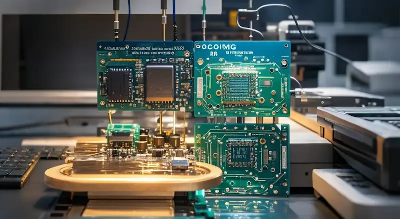

When discussing AI hardware, the spotlight almost always shines on 3nm chips, CoWoS advanced packaging, or HBM memory. However, as the "iceberg model" from Yole Group's PCB Industry 2026 Report reveals: the visible chips are only the tip of the iceberg. Hidden beneath the surface is the massive PCB and materials ecosystem that physically supports them. If you view the PCB industry through a traditional lens, you will miss a dramatic divergence currently unfolding. Today, from the perspective of a manufacturer, AnyPCBA explores how AI is reshaping the industry along two distinct paths.
Farewell to "Average Growth": The Polarization of the PCB Market
In the past, the industry was accustomed to evaluating the PCB market using an average compound annual growth rate (CAGR) of around 8.1%. But this is a highly misleading metric. Behind the overall $88 billion market size lie two completely different trajectories:
AI-Related High-End Boards: CAGR of 45% to 70%.
Standard General-Purpose Boards: Growth is nearly stagnant.
Value is shifting rapidly. Data shows that by 2031, the annual growth rate for 18+ layer high-end PCBs will reach 15.7%, while 4-6 layer standard boards will grow at only 2.3%. Since 2020, the share of servers and data centers in PCB demand has risen from 16% to 25%, officially replacing consumer electronics as the strongest engine for PCB growth.
The Core Driver: Surging System Value and the "Semiconductorization" of PCBs
In this AI wave, the growth of the PCB market is not simply driven by shipping more units, but by the explosive increase in the "value per system."
Take NVIDIA's next-generation racks (including the Vera Rubin platform) as an example: the corresponding PCB value has surged by over 200%, with 57% of that increment coming from entirely new board categories that did not exist in the previous generation. In AI servers, the proportion of ASICs is rising, and the PCB value of a custom accelerator is roughly twice that of a GPU.
Why are boards getting so expensive? Because the circuit board is taking on the functions of a package.
At ultra-high speeds of 224 Gbps, the skin depth is only about 0.27 micrometers. Copper surface roughness, which was negligible in the previous generation, now directly causes severe signal loss. This confirms the industry trend of "PCB semiconductorization"—the iteration cycle of copper-clad laminates (CCL) has synchronized with chips. From M7 materials for GB300 to M8 for Vera Rubin, and future M9 and M10 platforms, each generation upgrades all four main materials. Consequently, the unit price of M9 materials has reached four times that of M7.
Automotive Electronics: The Second Growth Curve for High-End HDI
Beyond AI computing, automotive electronics is another powerful growth engine. The automotive PCB market is expected to exceed $23 billion by 2031.
However, this is also accompanied by structural shifts: PCB demand for traditional internal combustion engine (ICE) vehicles is shrinking by 15% annually. In contrast, PCBs for EV powertrains are growing at 30%, and central computing boards for Advanced Driver Assistance Systems (ADAS) are growing at an impressive 46%. Even after cloud capital expenditures normalize, the intelligent upgrade of the automotive sector will continue to drive massive demand for high-end HDI boards.
The AnyPCBA Perspective: Bridging the Gap Between Design and Advanced Manufacturing
With the explosion of 18+ layer boards, M8/M9 high-speed materials, and ultra-fine traces, hardware teams face not just design challenges, but significant manufacturing and supply chain gaps.
As a seasoned PCBA manufacturer, AnyPCBA provides critical support for hardware clients navigating these cutting-edge trends:
Advanced Manufacturing Capabilities: To meet the demands of AI servers and high-performance computing, AnyPCBA supports high-layer-count boards up to 64 layers. We possess mature HDI (High-Density Interconnect) and Rigid-Flex capabilities, perfectly matching the complex stack-ups of server compute boards and new accelerator modules.
High-Frequency Material Processing: Facing the iteration of M7/M8 and higher-grade materials, AnyPCBA has extensive experience in High-Frequency Hybrid stack-ups. We strictly control impedance and ultra-low loss requirements to solve signal integrity challenges in the 224 Gbps era.
Precision Impedance & Warpage Control: As PCBs evolve toward semiconductor-level complexity, trace widths approach physical limits. AnyPCBA's DFM team conducts rigorous simulation and process reviews before production to ensure the lamination yield of ultra-low roughness copper foils and the thermal stability of multilayer structures.
Conclusion
AI is polarizing the PCB industry, but high-end manufacturing is never built overnight. When new board categories emerge and CCL cycles accelerate, you need a partner who understands both the trends and the manufacturing floor.
If you are developing next-generation AI computing, data center, or smart automotive hardware, contact the AnyPCBA team today. Let us back your advanced designs with highly reliable manufacturing processes.