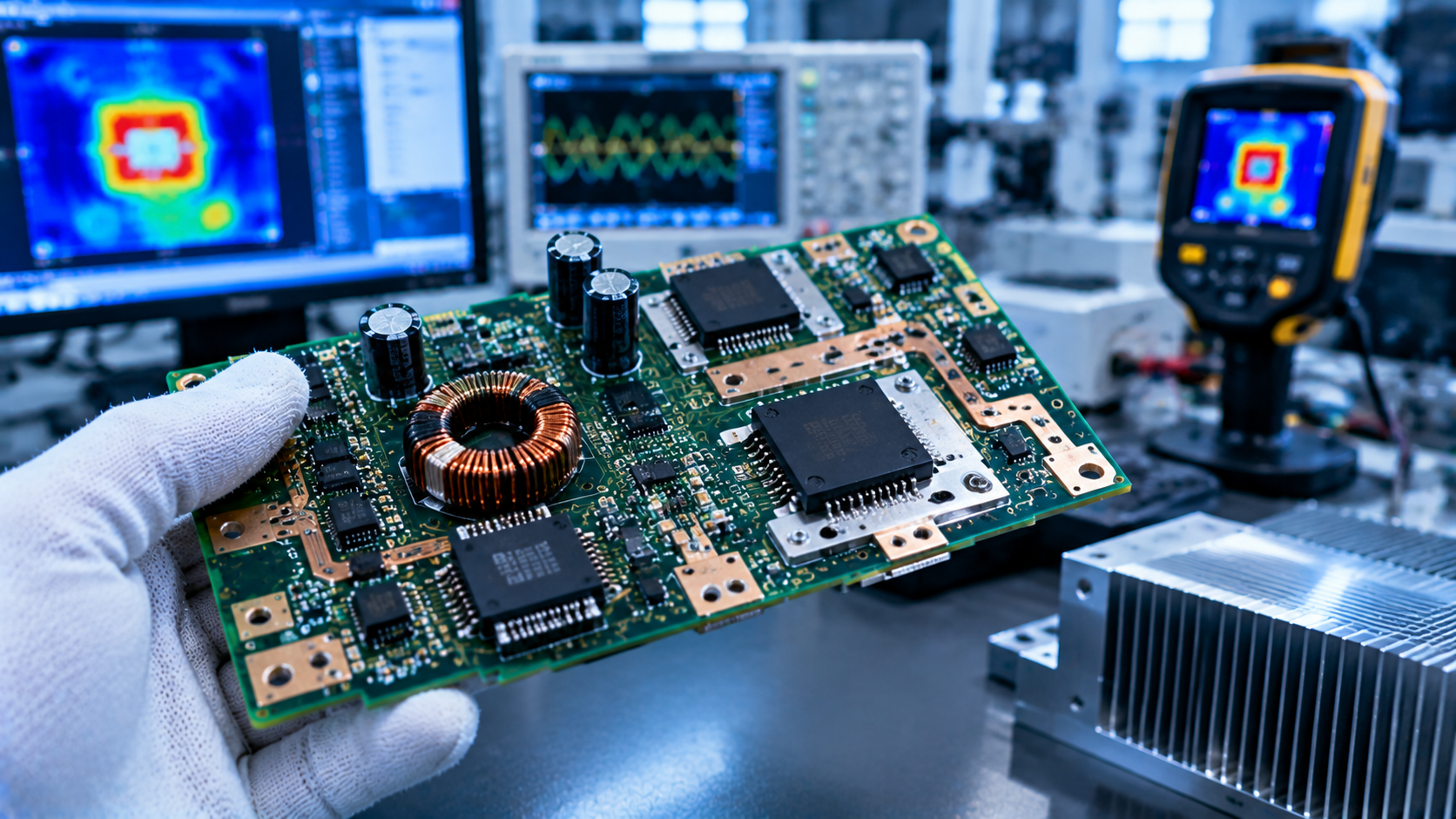
Introduction: High-power PCB design is more than connecting components. It requires balancing thermal management, EMC, signal integrity, power integrity, component placement, and routing—all within tight space and cost constraints. This article explains why engineers with this combination of skills are rare, and what manufacturing-side factors they need to understand.
Description: Based on AnyPCBA's small-to-medium volume PCB and PCBA manufacturing experience, this guide explains why high-power PCB design is a rare skill set—and how manufacturing-side factors such as copper distribution, etching tolerances, thermal relief, and depanelization stress affect real-world performance.
In the world of electronics engineering, high-power PCB engineers are like hidden superheroes. They use circuit boards as their canvas and electronic components as their paint, drawing the powerful heart that drives modern technology.
Yet when companies try to find such talent, they often discover the market seems short on people with these skills. Is it really that hard to find an engineer who excels at high-power PCB design?
The answer lies in the unique nature of high-power PCB design itself.
High-power PCB design is not simply about connecting electronic components. It is a fusion of technology and art.
Engineers must skillfully arrange power, signal, and ground within limited space while ensuring circuit stability and efficiency. It is like performing precision surgery—every detail matters.
It also demands that engineers understand five dimensions of constraints: thermal, electromagnetic, signal, layout, and routing. These five dimensions are not independent—they are coupled and mutually constraining.
One of the main challenges of high-power devices is heat dissipation.
Engineers must design the board's thermal path like a choreographer, choosing appropriate thermal materials, designing effective heat dissipation structures, and even using liquid cooling systems when necessary.
Thermal simulation software becomes an indispensable tool, using simulation and analysis to predict thermal behavior under various operating conditions.
The manufacturing perspective: At AnyPCBA, we see many high-power designs that perform well in thermal simulation but still run into problems in actual manufacturing. The reason often lies in copper distribution—copper is a thermal "highway," with thermal conductivity about 1300 times that of FR-4. Designers assume copper is uniform in simulation, but in actual manufacturing, copper distribution is affected by the etching process. Heavy copper boards also require special differential etching techniques to avoid side etching. These manufacturing variables are often simplified in simulation models.
In high-power devices, electromagnetic interference (EMI) is an issue that cannot be ignored.
Engineers need to act as guardians, protecting the circuit from external interference while ensuring the device does not interfere with other electronic equipment. This requires considering shielding, filtering, and grounding EMC measures during design, as well as skillfully arranging sensitive components and high-speed signal lines in the PCB layout.
The manufacturing perspective: EMC performance depends not only on design but also on manufacturing. Solder mask thickness consistency, surface treatment uniformity, and ground via fill quality all affect EMC performance. During DFM review, we specifically check ground via design to confirm whether plugging is needed and whether special surface treatment is required.
Signal integrity and power integrity are two key factors in high-power PCB design.
Engineers must ensure signal transmission in the circuit is clear and accurate, while power supply is stable and noise-free. This requires deep knowledge of electronic theory and a thorough understanding of high-speed digital and analog circuits.
The manufacturing perspective: There is often a gap between SI/PI simulation results and actual manufactured boards. The reason is manufacturing tolerances—trace width tolerance, dielectric thickness tolerance, copper thickness tolerance, and Dk variation. Designers use "nominal values" in simulation, while actual manufacturing produces values "within tolerance range."
In high-frequency, high-speed designs, this deviation can directly affect impedance and signal quality. So designers should account for manufacturing tolerances in simulation, rather than assuming manufacturing is perfect.
In high-power PCB design, component placement is critical.
Engineers need to think like strategists, considering the relative positions of components to reduce electromagnetic interference and thermal effects. At the same time, they need to consider the physical dimensions and mounting requirements of components, ensuring board manufacturability and maintainability.
The manufacturing perspective: Component placement affects not only electrical performance but also manufacturability directly.
A typical example is depanelization stress. If MLCC capacitors are too close to the depanelization line, mechanical stress during separation can crack them. This problem is invisible in electrical simulation but very common in manufacturing. During DFM review, we check the distance between components and the depanelization line and suggest layout adjustments when necessary.
Another example is thermal relief design. If a high-power device pad is directly connected to the ground plane without thermal relief, soldering becomes difficult because heat dissipates too quickly to reach sufficient soldering temperature—resulting in cold joints.
Routing is the art of PCB design. Engineers must skillfully arrange power, signal, and ground lines within tight space while avoiding line crossings and loops. They must be familiar with various routing rules and techniques, such as serpentine routing, differential pair routing, and impedance matching, to ensure circuit performance and reliability.
The manufacturing perspective: The boundary of routing technique is the factory's process capability.
Heavy copper boards (2oz and above), commonly used in high-power designs, require special differential etching techniques to avoid side etching. If the designer's trace width and spacing are too close to the factory's capability limits, yield cannot be guaranteed.
In addition, high-current traces in high-power designs need to consider current carrying capacity. A 1oz copper, 1mm trace can carry approximately 2A with a 10°C temperature rise. If the designer's current estimate doesn't account for temperature rise, the trace may overheat.
Back to the original question: is it really hard to find engineers who excel at high-power PCB design?
From the manufacturing side, what's hard is not "being able to draw a high-power board," but understanding electrical performance, thermal management, EMC, manufacturing processes, and supply chain at the same time.
An excellent high-power PCB engineer needs to:
Understand electrical principles and circuit topology
Master thermal simulation and EMC simulation tools
Be familiar with manufacturing process boundaries and limitations
Communicate effectively with the manufacturing side
Make trade-offs between cost, performance, and reliability
These abilities are not gained simply by operating EDA software. They require engineering judgment.
At AnyPCBA, we serve small-to-medium volume PCB and PCBA projects from 5 to 5000 pieces. High-power PCB is one of our common application scenarios, covering industrial power supplies, motor drives, automotive electronics, and photovoltaic inverters.
Our manufacturing capabilities cover 2 to 64 layers, supporting heavy copper (2oz to 20oz), HDI, rigid-flex, and high-frequency hybrid. We hold ISO 13485 (medical) and IATF 16949 (automotive) certifications.
During DFM review, we focus on:
Current carrying capacity and temperature rise estimation for high-current traces
Etching process windows and trace width tolerances for heavy copper boards
Manufacturability of thermal relief and thermal via designs
Pad dimensions and thermal paths for power devices
Impact of depanelization stress on components
Whether ground via and shielding designs meet EMC requirements
Our engineers help you judge these manufacturing risks at the design stage, so your high-power boards are not only drawable, but stable and reliable to produce.
If you're working on high-power PCB design, or want to learn more about our heavy copper and high-power manufacturing capabilities, contact us through our website.
What challenges have you encountered in high-power PCB design? Share your experience in the comments.




