Custom PCB Made to Order: A Comprehensive Guide for Your Project
In today's rapidly advancing technological landscape, custom printed circuit boards (PCBs) are the backbone of countless electronic devices. Whether you're an engineer prototyping a new invention or a company developing a product, having PCBs made to order provides the flexibility and precision needed for success. This guide dives into the process of obtaining custom PCBs, exploring key considerations and offering expert advice to ensure your project's success.
Understanding Your PCB Made to Order Needs
Before initiating a custom PCB order, a precise definition of project specifications is crucial. This ensures the final product aligns perfectly with the intended application, preventing costly redesigns and delays. This initial step involves a detailed assessment of various electrical and mechanical requirements.
- Layer Count
The number of conductive layers within the PCB significantly impacts its complexity and functionality. Choose the appropriate layer count based on your design's routing and signal integrity requirements, ranging from single-layer boards for simple circuits to multi-layer boards for complex applications. - Material Selection
The base material of the PCB influences its electrical and mechanical properties. Common materials include FR-4, known for its balance of cost and performance, and specialized materials like Rogers for high-frequency applications. Material selection affects dielectric constant, thermal performance, and mechanical strength. - Board Dimensions
Accurately specify the board's length and width to ensure it fits within the intended enclosure and interfaces with other components. Precision in dimensions is critical for mechanical compatibility. - Impedance Control
For high-speed circuits, controlling impedance is crucial to maintain signal integrity and prevent signal reflections. This requires specifying trace widths and spacing to match the required impedance for the application. - Copper Thickness
The thickness of copper layers affects the PCB's current-carrying capacity. Choose the appropriate copper thickness to support the required current flow and minimize heating. - Surface Finish
The surface finish protects copper traces from oxidation and provides a solderable surface. Common options include HASL (Hot Air Solder Leveling), ENIG (Electroless Nickel Immersion Gold), and OSP (Organic Solderability Preservative). Select a finish compatible with your soldering process and environmental requirements. - Via Types
Define the types of vias required, including through-hole vias, blind vias, and buried vias. The type of via selected depends on the number of layers and routing requirements.
Selecting the Right PCB Manufacturer
Choosing the appropriate PCB manufacturer is a crucial step in bringing your electronic design to life. This involves a careful evaluation of their capabilities, production speed, and cost-effectiveness to align with project needs. Key considerations include not only the technical expertise and manufacturing capacity but also their responsiveness, support, and overall reliability in delivering custom PCBs.
| Factor | Description | Importance |
|---|---|---|
| Technical Capabilities | Layer count, material options, minimum trace/space, via types, impedance control. | Critical for meeting specific design requirements. Ensures the manufacturer can accurately produce your PCB design. |
| Turnaround Time | Time from order placement to delivery, prototyping speed vs. mass production speed. | Crucial for project timelines. Quick-turn options are vital for prototyping; mass production requires scalable speed. |
| Pricing Structure | Cost per board, setup fees, tooling costs, assembly costs. | Directly affects project budget. Must balance cost with quality. |
| Minimum Order Quantities (MOQ) | Small-batch options vs. large-scale production. | Important for prototyping and smaller projects. Large MOQs may be unsuitable for early-stage projects. |
| Service Offerings | Prototyping, assembly, stencils, design support. | Can streamline the production process. Full-service manufacturers offer convenience. |
| Quality Control Standards | Certifications (e.g., ISO), testing capabilities, defect rate. | Ensures the PCB meets quality requirements. Low defect rate reduces overall project risks. |
| Customer Support | Responsiveness, communication channels, technical support. | Important for resolving issues and ensuring smooth production. |
The PCB Design Process: From Idea to Gerber Files
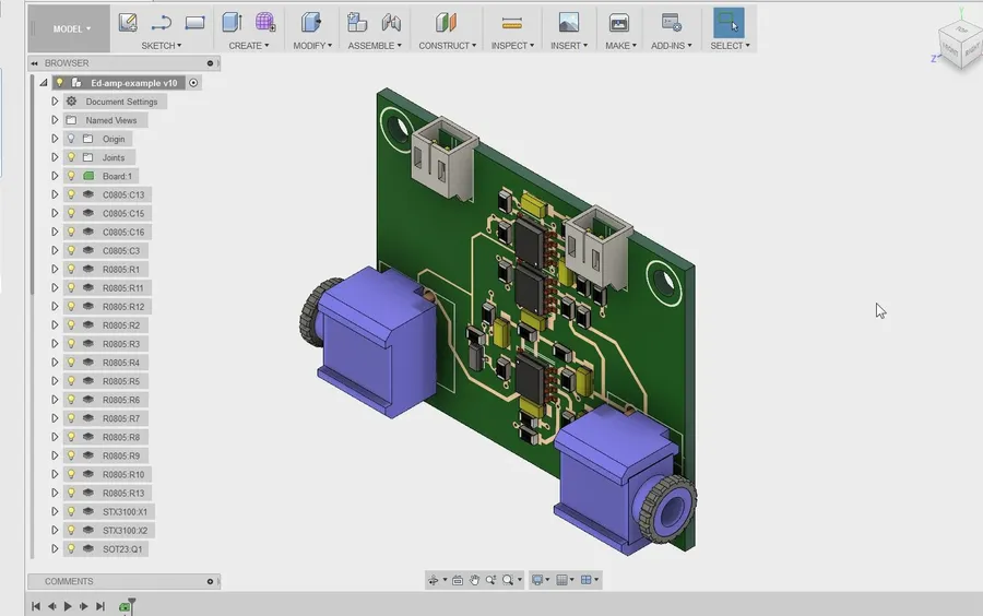
The journey from a conceptual idea to a manufactured Printed Circuit Board (PCB) is a multi-stage process that demands precision and adherence to established engineering practices. This process begins with a schematic capture, progresses to PCB layout, and culminates in the generation of Gerber files, which serve as the blueprint for manufacturing. Employing professional PCB design software and adhering to rigorous Design Rule Checks (DRC) are vital for ensuring the final product meets functional and quality standards.
- Schematic Capture
This is the initial step where the electrical design is captured using symbols for components and lines for connections. The schematic serves as a logical representation of the circuit, focusing on functionality rather than the physical arrangement. - PCB Layout Design
Once the schematic is complete, the physical layout of the PCB is designed, including the placement of components and the routing of traces. Considerations for factors like heat dissipation, signal integrity, and manufacturing constraints are critical at this stage. - Gerber File Generation
The final step is generating Gerber files, which are standard data formats containing all the necessary information for manufacturing the PCB, including layer data, drill data, and solder mask information. These files act as the universal language of PCB fabrication. - Design Rule Checks (DRC)
Throughout the process, and especially before generating Gerber files, DRC is essential. It is a system of automated checks that ensures the design meets manufacturability and performance criteria, preventing common issues like overlapping traces or insufficient spacing.
| Design Stage | Description | Key Considerations |
|---|---|---|
| Schematic Capture | Creating a logical circuit diagram | Component selection, logical connections, functionality |
| PCB Layout | Physical arrangement of components and traces | Component placement, trace routing, thermal management, signal integrity, manufacturability |
| Gerber File Generation | Exporting manufacturing files | Accuracy, completeness, standard format compliance |
| Design Rule Checks | Automated verification of design rules | Trace spacing, clearance, manufacturability, performance |
Navigating Online PCB Ordering Platforms
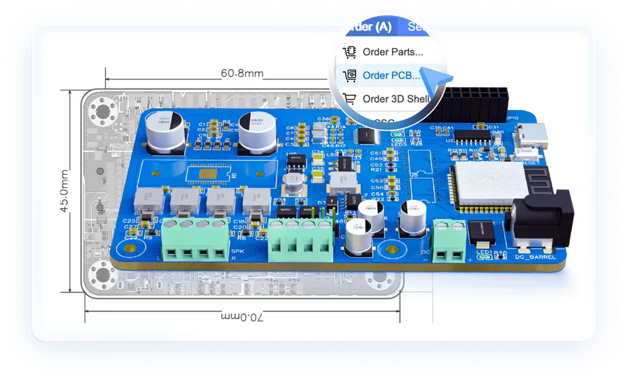
Online platforms have revolutionized the process of ordering custom PCBs, offering streamlined workflows for instant quotes, design file uploads, and manufacturing option selection. Understanding how to effectively use these platforms is crucial for a successful PCB made-to-order project.
These platforms typically provide a user-friendly interface where users can specify their PCB requirements, such as dimensions, layer count, material, and finish. After uploading the Gerber files, users can receive instant quotes, choose various manufacturing options, and place orders efficiently.
| Feature | JLCPCB | PCBWay | DigiKey |
|---|---|---|---|
| Instant Quotes | Yes | Yes | Yes (limited) |
| File Upload | Gerber, CAD | Gerber, CAD | Gerber |
| Manufacturing Options | Wide | Wide | Standard |
| Prototyping | Yes | Yes | Limited |
| Assembly Service | Yes | Yes | No |
| Turnaround Time | Fast | Fast | Standard |
| Pricing | Competitive | Competitive | Higher |
When choosing a platform, consider factors like ease of use, customer support, the variety of options available, and most importantly, whether they are capable of manufacturing your specific design. It is advisable to start with a few test runs before scaling production.
Cost Factors for Custom PCBs
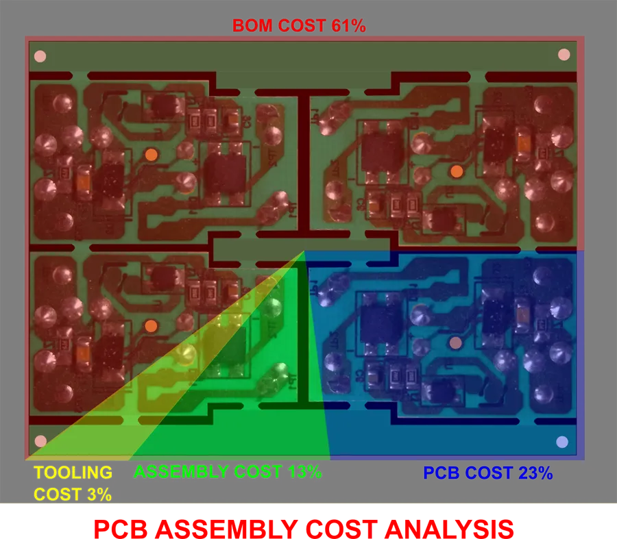
Understanding the cost drivers behind custom PCB fabrication is crucial for effective project planning and budgeting. Several interconnected factors influence the final price of a printed circuit board, with board size, layer count, material selection, and manufacturing complexity being the most significant. Optimizing these factors, where possible, can lead to substantial cost reductions.
| Cost Factor | Description | Impact on Cost |
|---|---|---|
| Board Size | The physical dimensions of the PCB. | Larger boards generally require more material and processing, increasing cost. |
| Layer Count | The number of conductive layers within the PCB. | More layers increase complexity and cost due to additional manufacturing steps. |
| Material | The substrate material used (e.g., FR-4, Aluminum, Rogers). | Specialty materials with high thermal conductivity or unique electrical properties command higher prices. |
| Manufacturing Complexity | Factors like minimum trace width, hole size, blind/buried vias. | Tight tolerances and complex designs necessitate more precise equipment and processes, adding to the price. |
| Surface Finish | The type of coating applied to pads and vias for soldering. | Gold (ENIG) is generally more expensive than HASL finish. |
| Quantity | Number of PCBs ordered in a single run. | Bulk orders typically have a lower per-unit cost due to economies of scale. |
| Turnaround Time | The speed at which the PCBs are manufactured and delivered. | Faster turnaround times often involve rush fees and higher per-unit costs. |
| Testing Requirements | The type and extent of testing required (e.g., flying probe, bed of nails). | Comprehensive testing increases cost due to additional time and resources spent. |
Additionally, it's prudent to compare pricing among different manufacturers, considering their capabilities and any additional services such as PCB assembly. Engaging manufacturers early to get quotes and design for manufacturability is vital to control costs.
Frequently Asked Questions About PCB Assembly and PCB Made to Order
This section addresses common inquiries regarding PCB assembly, focusing on aspects relevant to 'PCB made to order' scenarios. Understanding these nuances is crucial for successfully navigating the complexities of custom PCB manufacturing and assembly.
- What is the typical cost of PCB assembly?
The cost of PCB assembly varies widely based on factors including the complexity of the design (number of layers, component density), the number of boards being assembled, the type of components (through-hole vs. surface mount), and whether the components are supplied by the manufacturer or the customer. Costs can range from a few dollars for simple boards to several hundred dollars or more for complex assemblies with many components. For PCB made to order, it's best to get a quote based on your specific design and volume requirements. - How do I order PCB assembly using Gerber files?
To order PCB assembly using Gerber files, you must first generate these files from your PCB design software. Gerber files contain the essential data for manufacturing the board's layers, solder mask, and silkscreen. You also typically need a bill of materials (BOM) specifying all components, their part numbers, and quantities, and optionally a centroid file (pick-and-place file) that specifies the X-Y coordinates for component placement. Once you have these files, you can upload them to a PCB manufacturer's website or online platform for a quote and to place your order. - Who are the major PCB suppliers for 'PCB made to order' projects?
Several major PCB suppliers specialize in 'PCB made to order' services, catering to both prototyping and larger production runs. Notable suppliers include JLCPCB, PCBWay, and DigiKey. These platforms offer various services from PCB fabrication to full turnkey assembly, allowing for a wide range of customization based on the user's needs. Each has specific strengths, such as quick turnaround times, specific manufacturing capabilities, or cost advantages at certain volumes. Choosing the right supplier depends heavily on the specific needs of your project. - Why are some PCB manufacturing services seemingly very low cost?
The low cost of some PCB manufacturing services is often due to a combination of factors. These can include mass production at large facilities, automation of manufacturing processes, use of standardized materials and techniques, and economies of scale. Furthermore, some manufacturers located in regions with lower labor costs and different environmental regulations can produce PCBs at a lower cost. However, extremely low prices might mean limitations on material choices, tolerances, quality control and testing processes, which need careful consideration depending on the application of the 'PCB made to order'. - What factors influence the complexity of custom PCB assembly?
The complexity of custom PCB assembly is primarily driven by several factors. These include: the density and type of components (e.g., fine-pitch components), the number of layers in the PCB design, the use of advanced assembly techniques (e.g., reflow soldering, wave soldering), the need for specific testing procedures (e.g., in-circuit testing), and the complexity of the overall design. More complex PCBs often necessitate more sophisticated machinery and highly skilled personnel leading to an increase in assembly costs and longer lead times. - Can I get a custom PCB assembled with all components already soldered?
Yes, many 'PCB made to order' services offer full turnkey assembly, where the manufacturer fabricates the bare PCB, sources all the required components, and then assembles them onto the board. This greatly simplifies the process for the customer, saving time and effort. However, it does typically result in a higher cost compared to assembling the board yourself or contracting a separate assembly service. This convenience is crucial for many, especially for complex assemblies. - What are the key considerations for selecting components for a 'PCB made to order' project?
When choosing components for your custom PCB, consider several critical factors. Firstly, the electrical specifications of components must match your circuit's requirements, ensuring they meet voltage, current, and frequency demands. Secondly, consider the physical size of components to accommodate your board space. The availability of components, their lifecycle, and cost also play a significant role. It's also vital to confirm if the components are easy to assemble, especially for SMT (Surface Mount Technology), and whether they can be sourced easily. Choosing reliable vendors ensures consistent quality and avoids delays.
Ensuring Quality Control and Testing for PCB Made to Order
Rigorous quality control and testing are paramount to ensure that PCBs manufactured to order meet the required specifications and perform reliably in their intended applications. This involves a multi-stage process, from initial inspections to final functional tests, designed to identify and rectify any deviations from the design or manufacturing standards. Effective quality control not only reduces costly failures in the field but also ensures the longevity and integrity of the end product.
- Visual Inspection
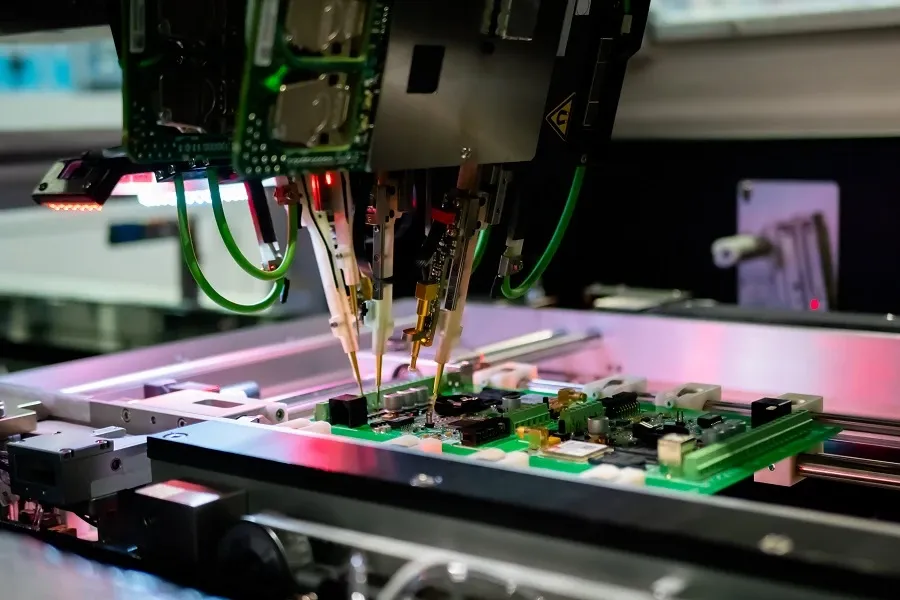
The first stage of quality control typically involves a visual inspection. This is a manual or automated check for any obvious defects such as improper solder joints, missing components, incorrect component placement, misaligned layers, or physical damage. High-resolution cameras and magnifying equipment are often used to detect these subtle imperfections. IPC standards, such as IPC-A-610, often provide the guidelines for acceptable visual quality. - Automated Optical Inspection (AOI)
Automated Optical Inspection (AOI) uses cameras to capture images of the PCB to compare with a known good board. This is a faster, less subjective and more consistent approach than manual inspection and can detect a wide range of defects such as shorts, opens, component misalignment, wrong component, and improper soldering. This method uses software to identify deviations from predefined design criteria. - Electrical Testing
Electrical testing verifies the PCB's functionality by checking for shorts, opens, and correct circuit behavior. Common testing methods include: In-Circuit Testing (ICT) which uses bed-of-nails fixtures to access specific points on the PCB to check for connectivity and component values and functional testing which involves simulating the intended application environment to ensure that the PCB meets performance standards. These tests can also be used to check for impedance control and signal integrity. - X-ray Inspection
X-ray inspection is used to examine internal layers and solder joints that are not visible through a surface inspection. It can detect defects like voids in solder, misaligned vias, and hidden component failures. This method is crucial for multi-layer boards and complex assemblies. - Microsection Analysis
Microsection analysis provides a cross-sectional view of the PCB. A small piece of the PCB is cut, polished, and examined under a microscope. This allows for examination of plating quality, layer alignment, trace width/spacing, via structure, and solder joint quality at a microscopic level. It is destructive but critical for verifying manufacturing processes and identify potential reliability issues.
If any defects are found, the PCBs may need to be reworked or scrapped. Traceability is crucial in this process. Many manufacturers use unique serial numbers or bar codes to track each board during the process. This is important for identifying problematic batches and implementing corrective actions. The end goal is to deliver a product that meets all specifications and operates reliably. It is vital to keep thorough records of all testing processes for continuous improvement and potential failure analysis.
Turnaround Time and Logistics of PCB Manufacturing
Efficient PCB manufacturing hinges on understanding turnaround time and logistics, especially for custom orders. Turnaround encompasses the time from design submission to the delivery of finished boards, while logistics involves the shipping and supply chain aspects. Managing these elements is crucial for project timelines and overall success, whether for a quick-turn prototype or a larger production run.
Turnaround times vary significantly among manufacturers and depend on factors like PCB complexity and order volume. Quick-turn services often prioritize speed but may come at a higher cost, while standard production runs require more time for processing. Logistical considerations include shipping methods, customs clearance, and inventory management, all of which can impact delivery schedules.
| Factor | Impact on Turnaround Time | Impact on Logistics |
|---|---|---|
| PCB Complexity (layer count, material) | Increased complexity extends turnaround time. | More complex boards may require specialized shipping. |
| Order Quantity | Small quantity orders might have faster turnaround; large orders can extend it. | Large quantities need detailed shipping planning and might require specialized carriers or freight options. |
| Manufacturer's Production Capacity | Manufacturers with high capacity can potentially offer quicker turnaround. | Production capacity influences logistics, where production volumes need to be matched by shipping and delivery resources. |
| Shipping Distance | Short distances can translate to quicker deliveries. | Longer shipping distances increase the potential for delays. |
| Customization (special finishes, assembly) | Customization or specialized assembly can extend time. | Customizations need to be correctly accounted for in shipping documents. |
| Supply Chain Management | A well-managed supply chain ensures availability of components and minimizes production delays. | Effective logistics involves understanding the source of materials, anticipating lead times, and having backup plans to avoid disruptions. |
Future Trends in PCB Made to Order
The PCB made to order landscape is continually evolving, driven by advancements in materials, manufacturing techniques, and environmental concerns. These trends promise to reshape how custom PCBs are designed, fabricated, and utilized in various applications. Understanding these future directions will be crucial for staying competitive and innovative.
- Advanced Materials
The push for higher performance and flexibility is leading to the adoption of advanced PCB materials such as ceramics, liquid crystal polymers (LCP), and specialized composites, offering superior thermal, electrical, and mechanical properties. These materials enable PCBs to operate at higher frequencies and in more demanding environments. - Flexible and Stretchable PCBs
Flexible PCBs, made from materials like polyimide, are gaining popularity in wearable devices and applications requiring non-planar geometries. The development of stretchable PCBs, utilizing conductive inks and elastic substrates, is pushing boundaries for integration into curved or dynamic surfaces. - Miniaturization and High-Density Interconnect (HDI)
The trend towards smaller and more densely packed electronic devices is driving the adoption of HDI technologies. This includes microvias, finer line widths, and advanced substrate materials, enabling more complex circuitry in smaller form factors. - Embedded Components
Embedding passive components like resistors, capacitors and even active components within the PCB layers further minimizes size and improves signal integrity. This integration leads to more compact and efficient electronic designs. - Sustainable and Eco-Friendly Manufacturing
Environmental awareness is increasing, leading to more sustainable manufacturing processes. This involves the use of eco-friendly materials, reduced chemical usage, and improved recycling methods for PCB waste. There's also growing interest in bio-based materials. - Additive Manufacturing (3D Printing)
Additive manufacturing or 3D printing of PCBs is gradually becoming a viable method for rapid prototyping and small production runs. This technology reduces the lead times, allowing for more complex geometries and enabling customized designs with ease. - Smart PCBs
Emerging trends include embedding sensors, microcontrollers, and other intelligent components directly into the PCB itself, enabling smart or interactive functionalities, from real-time monitoring to adaptive system response.
Obtaining a PCB made to order is a critical process that demands careful planning and execution. By understanding the intricacies of design, manufacturing, and supplier selection, you can ensure a successful outcome. Whether you are a hobbyist working on a small project or a large company launching a new product, the right approach to custom PCB design and manufacturing is key to your success. Looking ahead, advancements in PCB technology and manufacturing will continue to transform how we use and interact with electronics. Embrace these changes, and you'll stay at the forefront of innovation.