Finding the Best Cheap Custom PCB: A Comprehensive Guide
In today's electronics-driven world, custom PCBs are the backbone of countless devices. But the cost can be a major hurdle. This article dives deep into finding the most affordable options for high-quality, cheap custom PCBs. We'll explore various manufacturers, their offerings, and cost-saving strategies to empower your electronic projects without breaking the bank, connecting technical needs with practical solutions.
Understanding the Factors Affecting PCB Costs
The cost of custom PCBs is influenced by a complex interplay of design and manufacturing choices. Understanding these factors is crucial for cost optimization without compromising the required functionality and quality of your printed circuit board. This section will delve into key determinants such as board dimensions, layer count, material selection (particularly FR-4 variations), surface finishes, and the impact of production volume on the final price.
- Board Size
Larger PCBs require more material and processing time, directly increasing costs. Optimizing the board size to fit your circuitry efficiently will help to minimize waste and cost. - Layer Count
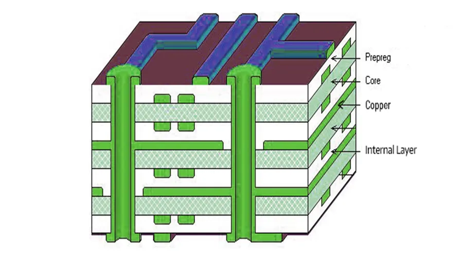
The number of conductive layers (single, double, multi-layer) significantly affects the manufacturing complexity and cost. Additional layers increase the cost substantially due to the extra material, processing steps and precision required. - Material Type (FR-4)
While FR-4 is a cost-effective material, variations such as standard Tg (glass transition temperature) and high-Tg FR-4 influence performance and cost. High Tg materials are more resistant to heat but are usually more expensive. - Surface Finish (HASL, ENIG)
The type of surface finish (e.g., HASL, ENIG, OSP) impacts both performance and price. ENIG provides better solderability and corrosion resistance but is more costly than HASL. The selection of surface finish should be based on design requirement and cost consideration. - Production Volume
The number of boards manufactured influences the unit cost. Larger production volumes can result in lower per-unit costs due to economies of scale. When ordering, consider the possibility of ordering in bulk.
Top Cheap Custom PCB Manufacturers Compared
Selecting the right PCB manufacturer is crucial for balancing cost and quality. This section provides a comparative analysis of leading budget-friendly PCB manufacturers, focusing on their capabilities, pricing, lead times, and customer feedback. The analysis will help you identify the ideal partner for your specific project needs, whether it’s prototyping or mass production.
| Manufacturer | Specialization | Price Range (USD/10 PCBs) | Avg. Shipping Time (Days) | Key Features |
|---|---|---|---|---|
| PCBWay | Prototype, Small Batch, Mass Production | 5-30 | 3-10 | Wide range of materials, advanced options, assembly service |
| JLCPCB | Prototype, Small Batch, Mass Production | 2-25 | 3-10 | Very competitive pricing, quick turnaround, good for beginners |
| Elecrow | Prototype, Small Batch | 8-35 | 5-12 | Good for small projects, offers component sourcing, and laser cutting service |
| ALLPCB | Prototype, Small Batch, Mass Production | 6-32 | 4-11 | Focus on quick turn, good for both prototypes and volume production. |
| OSH Park | Prototype, Small Batch | 10-40 | 10-15 | High quality prototype service, purple boards |
Material Options and Their Impact on PCB Cost
The choice of materials in Printed Circuit Board (PCB) manufacturing significantly influences both the performance and cost of the final product. Selecting the appropriate material is crucial for balancing functionality and budget. This section will primarily focus on FR-4, the most commonly used material, while briefly touching on other options like aluminum and flexible substrates.
FR-4 (Flame Retardant type 4) is a composite material consisting of woven fiberglass cloth with an epoxy resin binder. It is favored for its balance of electrical performance, mechanical strength, and cost-effectiveness. The cost of FR-4 boards is influenced by its thickness, copper weight, and the type of epoxy resin used. Within FR-4 there are also variations in the Tg temperature, which will be covered in more detail.
| Material | Description | Typical Applications | Cost Considerations | Advantages | Disadvantages |
|---|---|---|---|---|---|
| FR-4 | Woven fiberglass with epoxy resin | Most general-purpose PCBs | Low to moderate; depends on thickness and Tg | Good balance of electrical/mechanical properties, cost-effective | Limited thermal performance, rigid |
| Aluminum | Aluminum core with dielectric layers | LED lighting, power electronics | Moderate to high | Excellent thermal conductivity, durable | Higher cost, less common, may not be suitable for all applications |
| Flexible Substrates (e.g., Polyimide) | Flexible polymer films | Wearable devices, flexible electronics | High | Highly flexible, lightweight | Higher cost, more difficult to process |
Within FR-4, the glass transition temperature (Tg) is a critical parameter. Standard Tg FR-4 typically has a Tg of around 130-140°C, suitable for most applications. High-Tg FR-4, with a Tg of 170°C or greater, provides enhanced thermal stability, and is suitable for applications that involve high temperatures during operation or assembly. High Tg FR-4 boards are more expensive than standard Tg boards.
For standard electronic products, FR-4 with a standard Tg is usually sufficient. However, when considering applications in harsh environments or with high temperature requirements, high-Tg FR-4 or Aluminum will be needed, although this will impact cost.
Surface Finish Choices and Their Cost Implications
The surface finish of a printed circuit board (PCB) is a critical aspect influencing its solderability, reliability, and ultimately, its cost. Selecting the appropriate finish requires careful consideration of project requirements and budget constraints. Different finishes offer varying levels of performance in terms of corrosion resistance, contact resistance, and compatibility with different soldering processes. This section details common surface finish options, their characteristics, and their cost implications to help you make an informed decision.
| Surface Finish | Description | Pros | Cons | Cost |
|---|---|---|---|---|
| HASL (Hot Air Solder Leveling) | A process where molten solder is applied and then leveled using hot air knives. | Low cost, good solderability, widely available. | Uneven surface, not suitable for fine pitch components, lead-free HASL may have reliability concerns | Low |
| ENIG (Electroless Nickel Immersion Gold) | A two-layer metallic finish where a layer of nickel is deposited, followed by a thin layer of gold. | Excellent solderability, good oxidation resistance, suitable for fine pitch components, flat surface. | Higher cost, potential for 'black pad' issues. | High |
| Immersion Silver | A thin layer of silver is deposited on the copper pads via a chemical process. | Good solderability, moderate cost, suitable for wire bonding. | Prone to tarnishing, requires special handling, less robust than ENIG. | Moderate |
| OSP (Organic Solderability Preservative) | A thin organic layer protects copper from oxidation, enhancing solderability. | Low cost, flat surface, good for reflow soldering. | Poor shelf life, sensitive to handling, poor contact surface. | Low |
When selecting a surface finish, prioritize the requirements of your project. For cost-sensitive applications and through-hole soldering, HASL is a practical choice. For fine pitch surface mount components where planarity is critical, ENIG is preferable, despite its higher cost. If you need a middle ground, Immersion silver offers a reasonable alternative. OSP is suitable for applications requiring low cost and a flat surface, but careful handling and quick assembly are critical. Always check with your manufacturer on the specific requirements for your board design, and consider if the finish aligns with the long term usage environment.
Strategies for Reducing PCB Manufacturing Costs
Reducing PCB manufacturing costs requires a multifaceted approach, combining design optimization, smart material choices, and leveraging manufacturer's capabilities. By strategically addressing each of these factors, significant cost savings can be achieved without compromising functionality or quality.
- Optimize Board Design
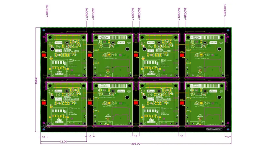
Simplify the PCB layout by using fewer layers, minimizing board size, and choosing components with smaller footprints where possible. Smaller board sizes directly reduce material consumption and manufacturing time. - Panelization
When ordering multiple PCBs, consider panelizing them. This involves combining multiple copies of your board into a single larger panel. This can lead to significant cost reduction per PCB as manufacturers often charge less for handling larger panels. - Bulk Ordering
PCB manufacturers generally offer price breaks for higher order volumes. If your project needs more than a few boards, consider ordering in bulk to lower the per-unit cost. Evaluate the overall project needs for cost-benefit analysis of bulk ordering including warehousing considerations. - Alternative Materials
While FR-4 is the most common, explore alternative materials if your application permits. Consider the performance implications and cost of standard FR-4 vs high-Tg FR-4 when making cost-benefit decisions. Choosing a lower-cost dielectric material can significantly affect cost. - Component Selection
Opt for cost-effective components with a high value proposition and consider using standard, readily available parts. Review datasheets carefully for component parameters, reliability and lifetime to ensure design intent. - Negotiate with Manufacturers
Do not hesitate to negotiate pricing with manufacturers, especially for large orders or repeat business. Explore discount and special offers from PCB manufacturers such as student discounts or bulk order discounts and plan projects to leverage these opportunities. - Early Supplier Engagement
Engaging with the PCB manufacturer early in the design process can help optimize the design for cost-effectiveness. This proactive collaboration can prevent costly revisions later on.
The Importance of Design for Manufacturing (DFM) to Reduce PCB Cost
Design for Manufacturing (DFM) is a crucial process in PCB production, focusing on optimizing designs to minimize manufacturing costs and prevent potential issues. By considering DFM principles during the design phase, significant cost savings and improved yield rates can be achieved.
DFM involves considering manufacturing capabilities and limitations early in the design process. Ignoring these considerations can lead to higher production costs, longer lead times, and even design revisions. A robust DFM approach ensures that the final PCB design is not only functional but also manufacturable in a cost-effective and efficient manner.
Key aspects of DFM include:
- Minimum Trace Width and Spacing
Ensure traces are wide enough and have adequate spacing to meet the manufacturer's capabilities and prevent shorts or open circuits. - Via Size and Placement
Choose via sizes that are within the manufacturer's capabilities. Avoid placing vias too close to pads or other features. - Pad Size and Shape
Use appropriate pad sizes and shapes to ensure reliable soldering. Consider component datasheets for recommended footprints. - Hole Sizes and Placements
Specify hole sizes that are within the manufacturing tolerances. Avoid placing holes too close to the board edge or other features. - Clearance Rules
Adhere to clearance rules between traces, pads, and other copper features to prevent shorts. Consult manufacturer specifications for recommended clearances. - Copper Balancing
Ensure even distribution of copper on each layer to prevent warping during manufacturing. - Solder Mask and Paste Layer Design
Optimize the solder mask and paste layers to ensure proper soldering and prevent solder bridging.
Gerber file checking is an integral part of the DFM process. Before sending designs to the PCB manufacturer, it's vital to review your Gerber files to verify all features are correctly represented and that they adhere to manufacturing specifications. This step will prevent costly issues during production.
Tips for Gerber file checking:
- Verify Layer Alignment
Ensure all layers are perfectly aligned. Any misalignment can result in manufacturing defects. - Check for Shorts and Opens
Carefully check for any unintentional shorts or open circuits in your design. - Confirm Drill Sizes and Locations
Verify that drill files correspond with your design. - Review Solder Mask and Paste Layers
Ensure that solder mask and paste layers are properly applied and do not overlap. - Check for Missing or Incorrect Features
Make sure all design elements, such as traces, pads, and vias, are present in the Gerber files.
Frequently Asked Questions About Cheap Custom PCBs
This section addresses common questions regarding the cost-effective manufacturing of custom PCBs. We aim to provide concise, insightful answers to help you navigate the options for your projects.
- What is the cheapest way to make a custom PCB?
The most cost-effective approach to PCB manufacturing involves optimizing your design for manufacturability, selecting a cost-effective material like standard FR-4, using a standard surface finish such as HASL, and ordering in bulk. Avoiding unnecessary complexity and utilizing panelization can significantly reduce costs. Additionally, choosing manufacturers based in regions with lower production costs, such as China, can make a substantial difference for smaller budgets. - What is the most cost-effective PCB surface finish?
HASL (Hot Air Solder Leveling) is generally the most economical surface finish. It's widely available and offers good solderability. ENIG (Electroless Nickel Immersion Gold) is more expensive due to the gold plating process, but provides better flatness and corrosion resistance but is not needed for most low cost applications. - How much does a single custom PCB typically cost?
The cost of a single custom PCB can vary significantly based on specifications, ranging from a few dollars for basic, small boards to several tens of dollars for more complex designs with multiple layers, specialty materials, and premium surface finishes. Prototype runs, especially for small quantities, tend to have higher per-unit costs due to setup and tooling. Bulk orders lower the per-piece price considerably due to economies of scale. - Why are custom PCBs sometimes so expensive?
Several factors contribute to the cost of custom PCBs, including: the number of layers, the type of materials used (e.g., high-Tg FR-4 or aluminum), the complexity of the design, the chosen surface finish, the quantity ordered, and the manufacturer's location. Specialized requirements such as impedance control and tight tolerances can also increase cost. One-off orders or small quantities typically face high per-unit costs because the manufacturing setup costs are spread over a small number of boards. - How does board size affect the cost of a custom PCB?
Larger PCBs typically cost more due to the increased material usage, production time, and processing complexity. Smaller boards tend to be more cost-effective, as they require less material and often simplify production. Optimizing PCB dimensions to fit a standard panel size can also minimize material wastage and production cost. - Can the number of layers significantly increase my PCB cost?
Yes, the number of layers directly impacts the cost. Each added layer increases the manufacturing complexity, process time, and material usage. Therefore, double-layer or four-layer PCBs are typically more cost effective compared to complex multi-layer designs. For simpler circuits, sticking to fewer layers can greatly reduce expense. - What is the impact of the PCB material on its final price?
The most commonly used material, FR-4, is a cost-effective choice for most applications. However, high-performance materials like high-Tg FR-4 (which tolerates higher temperatures), aluminum-backed PCBs, or flexible substrates will increase the cost due to their higher material expense and more complex manufacturing process. If performance requirements allow, FR-4 is the best option for cost-sensitive projects.
Understanding PCB Turnaround Time and Its Effect on Cost
PCB turnaround time, the duration from order placement to receiving the finished boards, significantly impacts manufacturing costs. Faster turnaround typically incurs higher expenses due to expedited production processes, while longer lead times often correlate with cost savings. This relationship is crucial for project planning, balancing project deadlines with budgetary limitations.
The trade-off between rapid prototyping and cost savings requires careful evaluation of project needs and priorities. For projects demanding quick verification of design concepts or rapid iterations, faster turnaround is beneficial and justifies the added cost, however, for projects with less urgent timelines, choosing a longer lead time can significantly reduce the overall cost. Understanding these trade-offs allows for optimized PCB production that aligns with project objectives and resource constraints.
- Standard Turnaround
Standard turnaround times typically range from a few days to a couple of weeks, depending on the manufacturer and the complexity of the PCB. This option is generally the most cost-effective for projects that do not have stringent time constraints. - Expedited Turnaround
Expedited or rapid turnaround services prioritize your order, reducing the manufacturing time to as little as 24-48 hours in some cases. This option is considerably more expensive but is often necessary for urgent prototypes, debugging or time-sensitive projects. - Factors Affecting Turnaround Time
Several factors impact the overall turnaround time, including board complexity (layer count, component density), material availability, current production backlog of the manufacturer, and surface finish requirements. Being aware of these can help in planning more accurately.
Actionable Table: Comparing PCB Manufacturers
Choosing the right PCB manufacturer is crucial for balancing cost and quality. This section provides a comparison table to help you make an informed decision based on your project's specific needs. Below is a side-by-side comparison of several popular PCB manufacturers, detailing their price ranges, average shipping times, and key features.
| Manufacturer | Price Range (USD) | Avg. Shipping Time | Key Features |
|---|---|---|---|
| PCBWay | Low to Medium | 3-10 days | Wide range of materials, assembly services, strong customer support, good for both prototype and small batch. |
| JLCPCB | Very Low | 3-10 days | Highly cost-effective for prototypes and small orders, SMT assembly available, large user base, strong for online ordering. |
| Elecrow | Low to Medium | 5-12 days | Offers PCB manufacturing, parts sourcing, and assembly services, good for one-stop solutions. |
| ALLPCB | Low to Medium | 5-12 days | Focus on rapid prototyping and quick turnaround times, offers a variety of manufacturing options. |
| OSHPark | Medium | 7-14 days | Specialized in small quantities and prototype, good for hobbyists, panelized orders, high quality. |
This table is designed to be an actionable tool, providing key insights to help you select the ideal manufacturer for your project. Remember to consider your specific design requirements, budget, and timeline when making your final choice. Note that the price ranges and shipping times provided are averages and can vary based on your specific requirements and the manufacturer's current workload. It's always best to get a quote based on your specific needs.
Finding the perfect balance between cost and quality is essential when ordering custom PCBs. By understanding the factors that impact PCB costs, choosing the right manufacturer, and implementing cost-saving strategies, you can produce high-quality, cheap custom PCBs that meet your project's needs without exceeding your budget. The future of electronics relies on accessible and affordable components, and knowing how to get a cheap custom pcb is the first step.