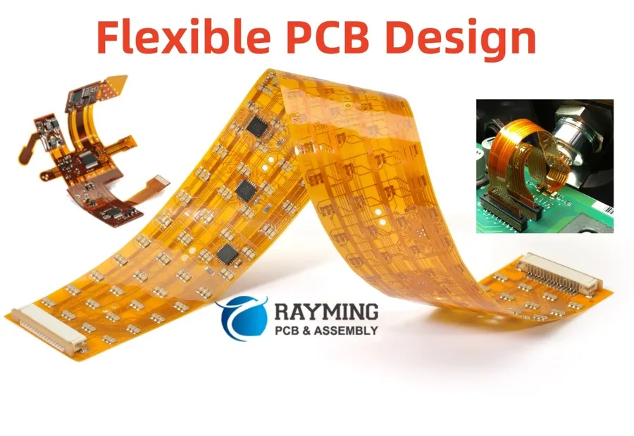
Flexible PCBs: The Ultimate Guide to Design, Materials, and Applications
In today’s rapidly evolving tech landscape, the demand for smaller, lighter, and more adaptable electronic devices is surging. Flexible PCBs, or flex circuits, emerge as a crucial solution, offering unparalleled design flexibility and reliability compared to traditional rigid boards. This article delves deep into the realm of flexible PCBs, exploring their core components, advantages, disadvantages, diverse applications, and the pivotal role they play in reshaping modern electronics. We'll connect you to the practical impact of these innovations in your day to day life, helping you understand the value of this technology.
What are Flexible PCBs?
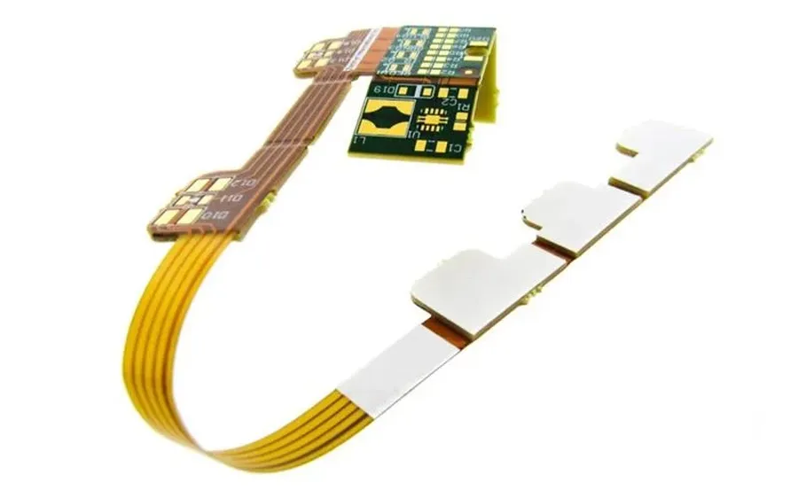
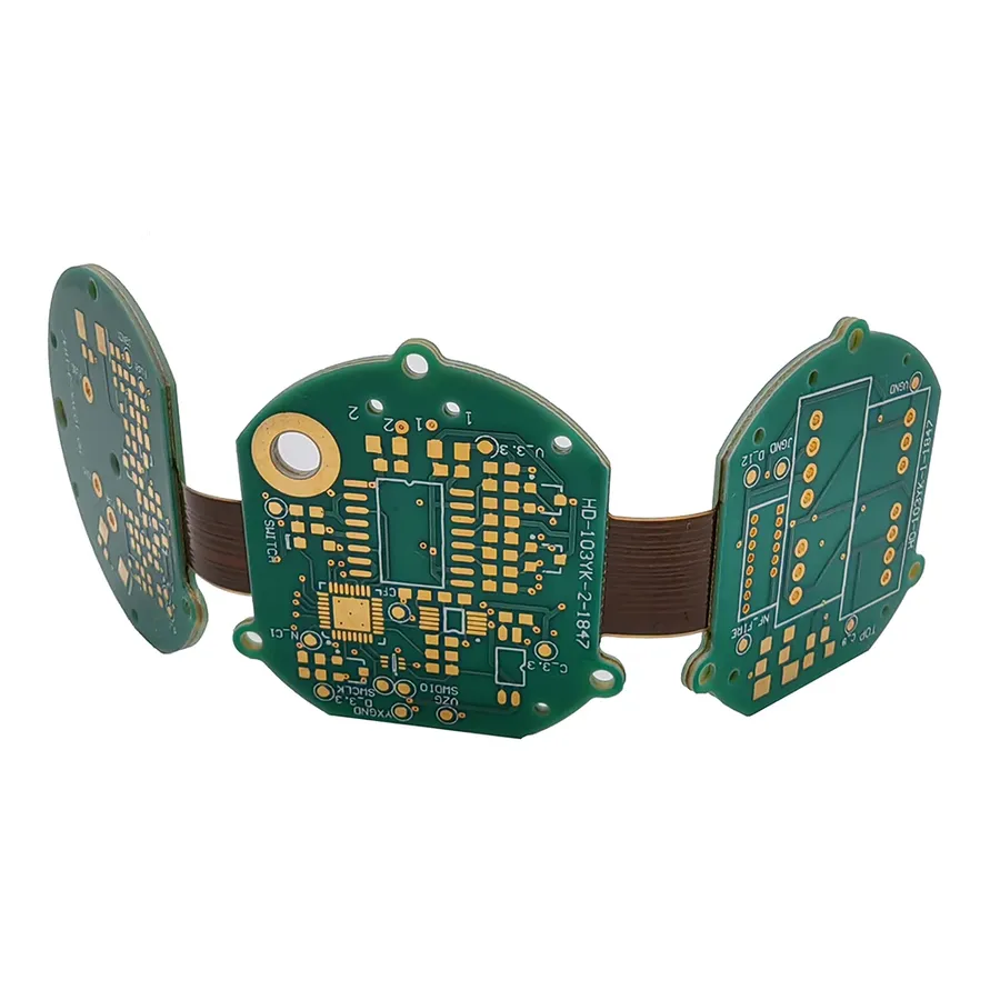
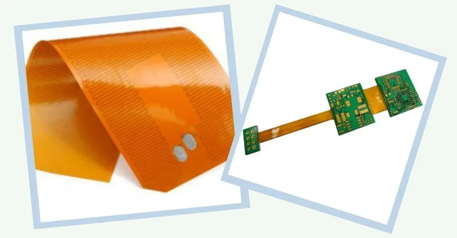
Flexible printed circuit boards (PCBs), often referred to as flex PCBs, represent a significant departure from traditional rigid PCBs. At their core, flex PCBs utilize flexible substrates, most commonly polyimide, to create circuits that can bend, fold, and twist, adapting to diverse spatial and mechanical requirements in electronic devices. Unlike rigid PCBs, which rely on inflexible materials like fiberglass epoxy, flex PCBs offer a dynamic and adaptable solution, enabling innovative designs and compact electronic assemblies.
The fundamental structure of a flexible PCB involves a thin, flexible dielectric substrate, often polyimide, onto which conductive copper traces are etched. These copper traces establish the electrical connections between electronic components. The entire assembly may include coverlays, adhesive layers, and stiffeners in specific areas to optimize the functionality and reliability of the circuit. This structure enables the flex PCB to maintain its electrical integrity even when subjected to bending or flexing.
Advantages of Flexible PCBs
Flexible PCBs offer significant advantages over rigid PCBs, primarily in applications requiring space optimization, dynamic movement, and enhanced reliability. These advantages stem from their inherent ability to conform to complex shapes and reduce the need for bulky connectors, ultimately leading to more compact and efficient electronic designs.
- Space and Weight Reduction
Flexible PCBs are significantly thinner and lighter than their rigid counterparts. This characteristic enables the design of smaller and lighter electronic devices, making them ideal for portable and wearable technology. - Design Flexibility
The flexible nature of these circuits allows for bending, folding, and twisting without compromising functionality. This adaptability facilitates complex and innovative designs that are simply not possible with rigid PCBs, enabling 3D packaging solutions. - Improved Reliability
By integrating components and interconnections directly onto a flexible substrate, the number of mechanical connectors can be dramatically reduced. This results in fewer potential failure points and improves overall system reliability and robustness, especially in dynamic or vibration-prone environments. - Reduced Assembly Time and Costs
The flexible nature of these circuits and reduction of connectors can simplify the assembly process, which decreases assembly time and costs. In some cases they can eliminate the need for wiring harnesses, streamlining manufacturing. - Dynamic Bending Capabilities
Flexible PCBs can endure repeated bending and flexing, making them suitable for applications with dynamic mechanical stresses, such as hinges, moving parts, or wearable devices that may undergo constant movement.
Disadvantages of Flexible PCBs
While flexible PCBs offer numerous advantages, it's crucial to acknowledge their limitations. These drawbacks often stem from their unique construction and the advanced manufacturing processes required, potentially impacting project feasibility and budget.
- Higher Initial Costs
Flexible PCBs generally have a higher per-unit cost compared to rigid PCBs. This is due to the specialized materials (like polyimide) and more intricate manufacturing processes required. The cost difference can be significant, especially for low-volume production runs. - Specific Design Requirements
Designing for flexible PCBs necessitates a different approach than rigid PCBs. Bend radii, trace routing, and component placement must be carefully considered to avoid stress and ensure long-term reliability. This increased complexity can lead to longer design cycles and a higher risk of errors if not handled meticulously. - Complex Manufacturing Processes
The fabrication of flexible PCBs involves more intricate processes compared to rigid PCBs. These include specialized handling, etching techniques, and lamination procedures specific to flexible substrates. This complexity can contribute to higher manufacturing costs and potential yield issues. - Component Mounting Limitations
Due to their flexible nature, flex PCBs can present challenges when mounting certain components. Large, heavy components may require additional support or reinforcement to prevent stress on the flex circuit. Furthermore, surface mount technology (SMT) processes may need specific adaptations to ensure reliable soldering on flexible substrates. - Repair and Rework Challenges
Repairing or reworking flexible PCBs can be more difficult than with rigid PCBs. The delicate nature of the flex material makes it more susceptible to damage during rework, requiring specialized equipment and techniques. This can lead to higher repair costs or a higher discard rate for faulty boards. - Material Sensitivity
Certain flexible substrate materials can be sensitive to environmental factors, like extreme temperatures or humidity. This sensitivity can limit their application in certain harsh operating environments and will demand careful material selection based on the intended application
Common Materials used in Flexible PCBs
The performance and reliability of flexible PCBs are significantly influenced by the materials used in their construction. These materials, primarily the substrate and conductive layers, dictate the mechanical, electrical, and thermal characteristics of the final product. This section details the most common materials, including their properties, advantages, disadvantages, and typical applications in flexible PCB manufacturing.
| Material | Properties | Advantages | Disadvantages | Typical Applications |
|---|---|---|---|---|
| Polyimide (PI) | High temperature resistance, excellent chemical resistance, good flexibility | High temperature stability, good dielectric properties, widely available | Higher cost compared to other substrates, can absorb moisture | High-reliability applications, aerospace, automotive, medical devices |
| Liquid Crystal Polymer (LCP) | Excellent dimensional stability, low moisture absorption, good electrical properties | Very low moisture absorption, excellent electrical performance at high frequencies, very good dimensional stability | Higher cost, limited availability | High-frequency applications, high-speed data transmission, RF modules |
| Polyester (PET) | Good tensile strength, low cost, good chemical resistance | Low cost, good flexibility, easy processing | Lower temperature resistance, poor chemical resistance to some solvents, less reliable than PI or LCP | Low-cost consumer electronics, disposable medical devices |
The selection of substrate material depends on the application's specific requirements. For instance, Polyimide (PI) is a robust choice for high-temperature environments and demanding applications because of its high-temperature stability and chemical resistance. Liquid Crystal Polymer (LCP), while more costly, excels in high-frequency applications because of its low moisture absorption and excellent electrical performance. On the other hand, Polyester (PET) offers a cost-effective solution for applications where temperature stability is less critical.
Copper is the primary conductor material, typically available in various thicknesses depending on the current requirements and the application. Common copper thicknesses range from 0.5 oz to 2 oz. Thinner copper is generally preferred for high-density applications where space is limited, while thicker copper is used in power distribution circuits with higher current requirements. Considerations such as the flexibility of copper traces and their susceptibility to fatigue under repetitive bending should be made in the design.
Material thicknesses are a crucial aspect of flexible PCB design. Substrates are available in different thicknesses, commonly ranging from 25 to 125 microns (1 to 5 mils). Thinner substrates provide greater flexibility but may have less mechanical strength, while thicker substrates provide more rigidity and mechanical robustness at the expense of flexibility. The thickness of the copper and the adhesive layers also contribute to the overall thickness and flexibility of the finished PCB. Careful consideration of the material thickness and layer stack-up is essential to achieving the desired performance and reliability of the flexible PCB.
Flexible PCB Design Considerations
Designing flexible PCBs (FPCBs) requires careful consideration of unique factors that differ from rigid PCB design. These considerations are crucial to ensure the functionality and reliability of the final product, encompassing aspects like bend radius, trace routing, stress management, component placement, and impedance control. Failure to account for these factors can lead to performance issues and premature failure of the flexible circuit.
- Minimum Bend Radius
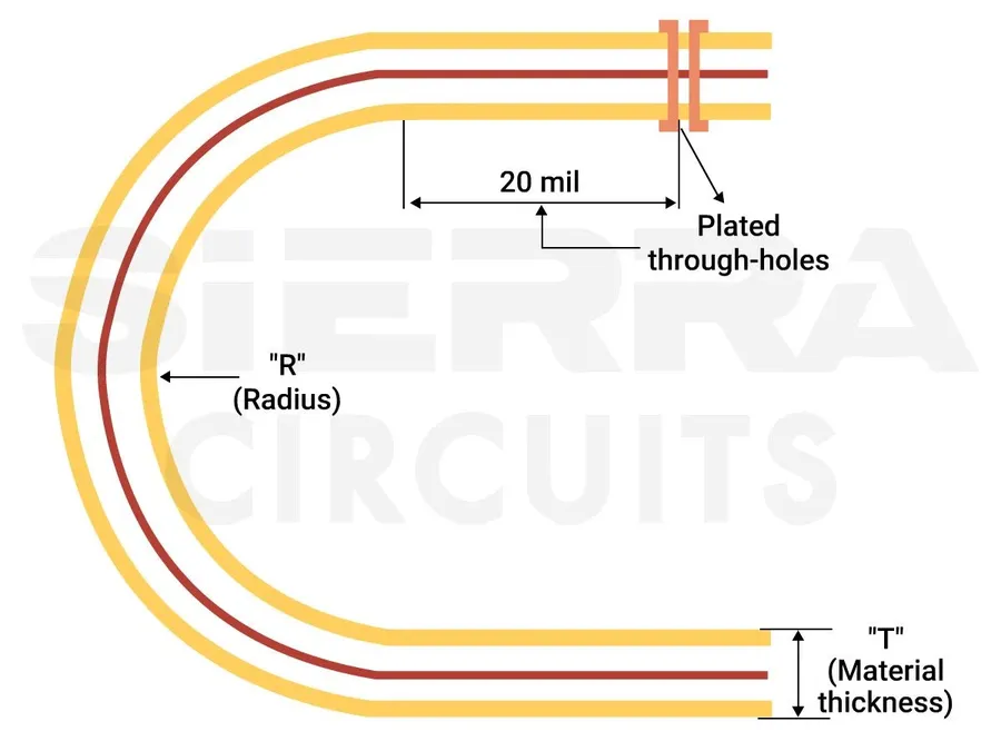
The minimum bend radius is the tightest curvature a flexible PCB can withstand without damage. This radius is primarily determined by the material properties and thickness of the flex PCB. Exceeding the recommended bend radius can cause stress and cracking of the conductor traces. Generally, dynamic bending applications require a larger bend radius than static applications. - Trace Routing
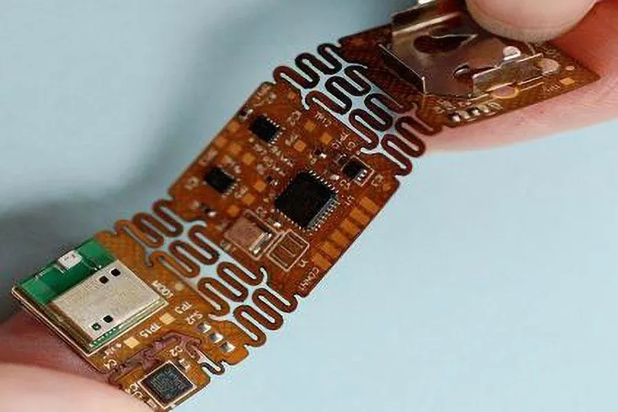
Trace routing on flexible PCBs needs to consider the bending and flexing. Traces should be oriented perpendicular to the bending direction whenever possible to reduce stress on the conductive lines. Using curved traces and avoiding sharp corners can help reduce stress concentrations. In areas subject to repetitive flexing, a thicker conductor or redundant routing may be required. - Stress Relief
Stress relief features, such as teardrops at trace junctions and larger pad sizes for components, are essential in preventing cracking and delamination. The use of fillets can also enhance mechanical strength. It is critical to identify high-stress areas and implement appropriate stress-relief techniques. - Component Placement
Component placement is critical for flexible PCB design. Components, especially heavier ones, should be placed in areas of minimal bending and flexing. Avoid placing components directly on or close to a bending area. In static bend applications components can be mounted closer to the bend location as long as suitable stress relief has been accounted for. In dynamic applications, components should always be positioned away from flex zones to maximize the mechanical reliability of the solder joints. - Impedance Control
Impedance control is just as critical in flexible PCB design as it is in rigid PCBs. Controlled impedance is necessary for high-speed signal transmission and proper signal integrity. Impedance variations can occur due to the bending and flexing of the PCB. Therefore, it is important to design the traces with the correct dimensions, and to pay careful attention to the dielectric properties of the FPCB. Ensure consistent trace widths and spacing across the entire circuit.
Flexible PCB Manufacturing Processes
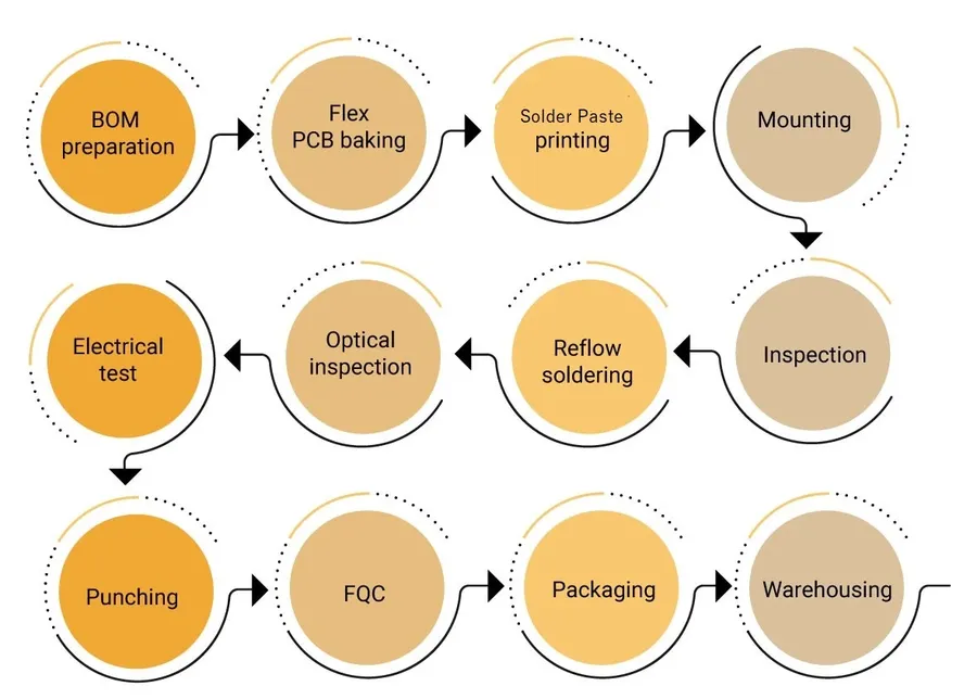
The manufacturing of flexible PCBs, or flex PCBs, involves a series of intricate steps that differ significantly from those used for rigid PCBs, primarily due to the flexible substrate material. These processes demand precision and careful handling to ensure the desired electrical performance and flexibility of the final product.
- Substrate Preparation
The process begins with the preparation of the flexible substrate, typically polyimide (PI), liquid crystal polymer (LCP), or polyester (PET). These materials are chosen for their flexibility, thermal stability, and electrical properties. The substrate is carefully cleaned and may undergo a surface treatment to enhance adhesion for subsequent layers. - Copper Cladding
A thin layer of copper is applied to the flexible substrate using techniques such as sputtering or electroplating. This copper layer will form the conductive traces of the PCB. The thickness and quality of the copper layer are critical for ensuring reliable electrical performance. - Circuit Patterning
Using photolithography, a precise circuit pattern is transferred onto the copper layer. A photosensitive resist is applied, exposed to UV light through a mask, and then developed, leaving behind the desired circuit pattern. This process requires high accuracy to match the design specifications. - Copper Etching
The exposed copper is etched away using chemical solutions, leaving behind the defined conductive traces. This step is crucial for achieving the desired electrical functionality and proper signal transmission. The etching process requires tight control to prevent undercutting or over-etching. - Lamination
In multilayer flex PCBs, additional layers of substrate and copper are laminated together using heat and pressure. This process requires precise alignment of layers and careful control of lamination parameters to ensure consistent and reliable layer bonding. - Drilling and Via Formation
Holes for through-hole components and vias for interlayer connections are drilled using mechanical or laser drilling techniques. These holes must be accurately positioned and sized to ensure proper component mounting and electrical connectivity. Laser drilling offers greater precision, especially for smaller features. - Surface Finishing
The final step involves surface finishing, which includes applying a solder mask to protect the circuit traces and a surface finish such as gold plating or ENIG (Electroless Nickel Immersion Gold) for enhanced solderability and corrosion resistance. These finishes are critical for reliable soldering and long-term durability. - Final Assembly
Once the fabrication of the flexible PCB is complete, components are mounted onto the board through processes such as surface mount technology (SMT). Quality control measures ensure components are placed correctly, and solder joints are robust. Further assembly may involve integrating the flex PCB into the final product, involving connectors or housings.
| Feature | Flexible PCB Manufacturing | Rigid PCB Manufacturing |
|---|---|---|
| Substrate | Flexible materials (e.g., polyimide, LCP, PET) | Rigid materials (e.g., FR-4, CEM-1) |
| Handling | Requires specialized handling due to flexibility | More robust handling processes |
| Lamination | More complex lamination processes for multi-layer flex | Standard lamination techniques |
| Drilling | May use laser drilling for precision vias | Primarily mechanical drilling |
| Cost | Generally higher cost due to material and process complexity | Lower cost due to standardized materials and processes |
Diverse Applications of Flexible PCBs
Flexible PCBs, owing to their unique blend of adaptability and performance, have permeated diverse industries, revolutionizing electronic design and integration. Their ability to conform to complex shapes, withstand dynamic bending, and reduce weight and space has made them indispensable in numerous cutting-edge applications.
- Consumer Electronics
Flex PCBs are integral to smartphones, tablets, laptops, and wearable devices. They connect components within these compact devices, facilitating intricate designs such as foldable screens and flexible displays. They also enable reliable button and sensor connections. - Automotive Industry
The automotive sector employs flex PCBs extensively in dashboard electronics, airbag systems, advanced driver-assistance systems (ADAS), and infotainment systems. Their ability to withstand vibrations, temperature variations, and tight spaces makes them ideal for automotive applications. - Medical Devices
Flex PCBs are vital in medical equipment including implantable devices, diagnostic tools, and patient monitoring systems. Their flexibility allows them to be used in minimally invasive devices, while biocompatible materials ensure patient safety. - Aerospace
In aerospace, flexible PCBs provide critical solutions for avionics, satellite systems, and aircraft controls. Their lightweight design and reliability under extreme environmental conditions are key to enhancing aerospace performance. They are frequently used in systems such as radar, navigation, and engine control units. - Industrial Automation
Flexible PCBs are employed in industrial automation equipment, including robotic arms, automated assembly lines, and sensor networks. They facilitate complex wiring within industrial machines, allowing for flexible movements and reliable signal transmission.
Frequently Asked Questions About Flexible PCBs
This section addresses common questions about flexible PCBs, providing concise and authoritative answers based on the principles discussed in previous sections. The intent is to clarify any uncertainties and offer a practical understanding of flexible PCB technology.
- What exactly is a flexible PCB?
A flexible PCB, often called a flex circuit, is a type of printed circuit board built on a flexible substrate material such as polyimide. Unlike rigid PCBs, they can bend and flex, making them ideal for applications requiring non-planar geometries or dynamic movement. - Can any PCB be made flexible?
No, not all PCBs can be made flexible. Traditional PCBs are constructed from rigid materials like FR-4. Flexibility is achieved by using specialized flexible substrates and conductive materials that can withstand bending and flexing without breaking the electrical connections. Only PCBs specifically designed and manufactured for flexibility using flexible base materials can be considered flexible PCBs. - What are the primary disadvantages of using flexible PCBs?
While offering significant advantages, flexible PCBs have some drawbacks. They typically involve higher initial manufacturing costs due to the materials and specialized processes required. They also have limitations in component mounting options and require more detailed design considerations compared to rigid PCBs. - Are flexible PCBs reliable for long-term use?
Yes, flexible PCBs can be very reliable when designed and manufactured correctly. The reliability of flexible PCBs depends greatly on factors such as the quality of materials used, proper bend radius design, and appropriate stress relief techniques. When these considerations are taken seriously, flexible PCBs can offer long-term stable performance and high reliability, even in dynamic environments. - How does the cost of flexible PCBs compare to that of rigid PCBs?
Generally, flexible PCBs have a higher upfront cost than rigid PCBs. This is largely due to the more expensive substrate materials, the precision manufacturing processes, and the often lower volume production runs. However, this higher cost can be offset in certain applications by the reduction in overall system weight and size, as well as elimination of connectors which can lead to a lower total system cost. - What are the typical materials used in the construction of flexible PCBs?
The most common material used in flexible PCBs is polyimide (PI), known for its excellent electrical and mechanical properties and resistance to heat and chemicals. Other materials include liquid crystal polymer (LCP) and polyester (PET), each having specific advantages for certain applications. The conductive layer is most often copper, sometimes with additional protective layers. - What design considerations are critical for flexible PCBs?
Several key design considerations include ensuring sufficient bend radius to avoid material stress, strategic trace routing to minimize signal degradation, effective stress relief mechanisms to prevent material tears or breakages, careful component placement, and precise impedance control. Proper planning is essential for optimal performance and long-term reliability.
Flexible PCB vs Rigid PCB: A Comparative Analysis
This section provides a detailed comparison between flexible PCBs and rigid PCBs, highlighting their distinct characteristics in terms of cost, applications, performance, design considerations, and suitability for various electronic products. Understanding these differences is crucial for selecting the appropriate PCB type for specific applications.
| Feature | Flexible PCB | Rigid PCB |
|---|---|---|
| Cost | Higher initial cost due to complex manufacturing processes and material costs. | Generally lower cost for basic designs, with cost increasing with complexity. |
| Applications | Ideal for applications requiring bending, folding, dynamic movement, or space constraints. Common in consumer electronics, automotive, medical devices, and aerospace. | Suitable for applications that do not require flexibility, such as computer motherboards, power supplies, and most general-purpose electronics. |
| Performance | Excellent for dynamic and static bending, with good signal integrity in flexible configurations. Can reduce the number of interconnections. | Stable performance in rigid configurations. Limited ability to conform to shapes or offer dynamic bending capabilities. |
| Design Considerations | Requires specific design considerations such as bend radius, trace routing for flexibility, and stress relief. Component placement is also a critical design aspect. | Design rules are generally less stringent but still important for signal integrity and thermal management. Component mounting is relatively straightforward. |
| Suitability | Well-suited for complex shapes, high-density connections, and applications with limited space. Excellent for dynamic applications. | Suitable for a wide range of general-purpose electronics where cost-effectiveness and rigidity are primary concerns. |
| Reliability | High reliability due to fewer interconnections and good vibration resistance when properly designed and manufactured | Reliability may be reduced by numerous connections which are prone to failure in harsh environments. |
Flexible PCBs represent a significant leap forward in electronics manufacturing, providing unmatched design flexibility and reliability. Their ability to adapt to complex shapes and harsh environments makes them ideal for a wide range of applications. As technology continues to advance, we can expect to see even more innovative uses for flexible PCBs, further blurring the lines between electronics and the objects they inhabit. Understanding the design, material, manufacturing and application aspects of flexible PCBs is crucial for engineers and designers looking to leverage the full potential of flexible circuit technology in cutting-edge products.