How to Order Custom PCBs: A Comprehensive Guide
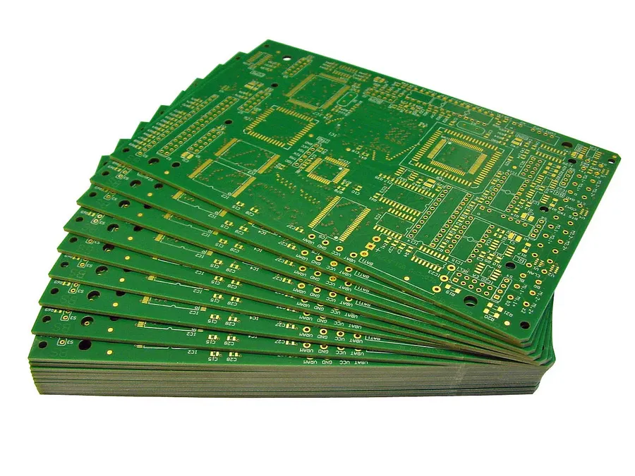
In today’s world of rapid innovation, custom PCBs (Printed Circuit Boards) are at the heart of almost every electronic device. From smartphones to sophisticated medical equipment, custom PCBs bring our ideas to life. If you are an engineer, a designer or a DIY enthusiast looking to order custom PCBs, this guide will lead you through each step to help you get your custom PCBs in a cost-effective and quick manner. The process can seem daunting, but with the right knowledge, it becomes a rewarding journey.
Understanding Your PCB Requirements Before You Order Custom PCB
Before initiating a custom PCB order, a thorough understanding of your project's specific requirements is paramount. This initial step ensures the final product aligns precisely with your needs, avoiding costly redesigns and delays. Defining these parameters accurately will guide you through the selection process, from choosing the right manufacturer to ensuring manufacturability.
- Board Dimensions
Precisely determine the required length and width of your PCB. Consider the overall size of your enclosure and the placement of other components. This is a critical factor for both functionality and manufacturability. - Number of Layers
Decide the number of conductive layers required for your circuit design (e.g., single-layer, double-layer, multi-layer). The complexity of your circuit and component density will influence this decision. - Material Selection
Choose the appropriate substrate material (e.g., FR-4, aluminum, flex). Consider factors such as thermal properties, mechanical strength, and dielectric constant to ensure optimal performance. - Special Features
Specify any unique requirements, such as controlled impedance, specific surface finishes, via types, or component footprints. - Component Placement and Spacing
Plan the locations and clearances for all your components, paying careful attention to tolerances and manufacturability. High density placements may require specific design rules
| Requirement | Considerations | Impact on PCB |
|---|---|---|
| Board Dimensions | Enclosure size, component placement | Manufacturing feasibility, component placement |
| Number of Layers | Circuit complexity, component density | Cost, signal integrity |
| Material Selection | Thermal, mechanical, electrical properties | Performance, reliability |
| Special Features | Impedance, surface finish, via types | Functionality, cost |
| Component Placement and Spacing | Tolerance, manufacturability | Manufacturing feasibility, cost |
Choosing the Right PCB Manufacturer to Order Custom PCB
Selecting the appropriate PCB manufacturer is a pivotal step in the custom PCB ordering process. This decision significantly influences the final product's quality, cost, and delivery timeline. A careful evaluation of various factors ensures that the chosen manufacturer aligns with your specific project requirements and budget constraints.
| Factor | Description | Considerations |
|---|---|---|
| Capabilities | The range of PCB specifications a manufacturer can handle, including layer count, materials, and minimum trace widths/spacing. | Ensure the manufacturer can produce PCBs meeting your design complexity. Check for special technologies (e.g., blind/buried vias, impedance control). |
| Price | The cost per PCB and the total cost of production. | Compare quotes carefully. Low prices might mean lower quality. Negotiate pricing for larger orders, also check for hidden costs like tooling and testing. |
| Turnaround Time | The time required to manufacture and deliver the PCBs. | Evaluate turnaround time relative to project deadlines. Express services might be available at an extra cost. |
| Customer Reviews & Support | Assess the manufacturer's reputation based on other users’ experiences. | Read online reviews and ratings. Look for responsiveness and the quality of customer support, check for post sale technical support. |
| Quality Standards | The manufacturing processes and the quality of finished PCB. | Verify if they are certified with ISO standards like ISO 9001. A proper system of inspection and testing during the manufacturing process is important. |
| Minimum Order Quantity (MOQ) | The minimum number of PCBs required for an order. | Some manufacturer do not have MOQ, while others do. Choose a manufacturer that aligns with you production volumes and scalability. |
| Location & Shipping | The geographical location of the manufacturer and shipping times. | Consider shipping costs, delivery times and customs duties. Local manufacturers might offer advantages in terms of delivery times and ease of communication. |
Preparing Your Design Files for Ordering Custom PCB
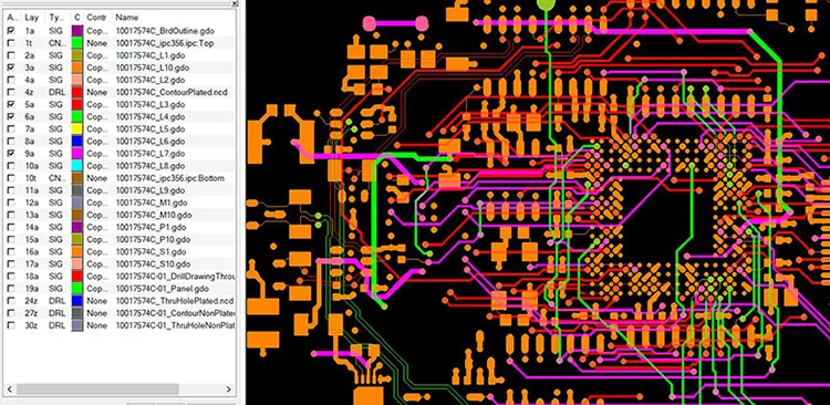
The accuracy and completeness of your design files are paramount for successful PCB fabrication. This section details the essential files required—Gerber files, Bill of Materials (BOM), and any other supplementary documentation—and provides guidance on their proper preparation and validation before submission to the manufacturer.
- Gerber Files
Gerber files are the industry standard for PCB fabrication. They are a set of 2D vector files that describe each layer of your PCB design, including copper traces, solder mask, silkscreen, and drill locations. Ensure all layers are correctly generated from your CAD software. - Bill of Materials (BOM)
A BOM is a comprehensive list of all components required for your PCB assembly. It should include component part numbers, manufacturer information, reference designators, and quantities. Verify that all components are available and accurately listed. - Pick and Place (PNP) File
When ordering assembled PCBs, a PNP file is essential for automated component placement. This file details the location and orientation of each component on the board. Confirm that the file is accurately exported from your CAD software and aligned with your BOM. - Additional Files
Depending on the complexity of your design or the requirements of your manufacturer, additional files may be required. This may include assembly drawings, special fabrication instructions, or specific layer stack-up details. Review the manufacturer's requirements carefully and provide all necessary documentation.
Before submitting your files, thoroughly validate them to avoid manufacturing delays or errors. This includes visual inspection of gerber files using a gerber viewer, cross-referencing components in BOM with schematic and PCB layout, and ensuring the PNP file matches the BOM and PCB design layout. Accurate and thorough documentation ensures a smooth fabrication process and reduces the likelihood of costly rework.
Comparing Quotes and Pricing for Order Custom PCB
Selecting the right PCB manufacturer involves a thorough comparison of quotes, extending beyond just the base price. Evaluating factors like quality, shipping costs, and lead times ensures that ordering custom PCBs aligns with your project's financial and temporal constraints. A comprehensive cost analysis is crucial for effective project management.
| Factor | Description | Impact |
|---|---|---|
| Base Price | Cost of the PCB itself, excluding additional fees. | Directly affects the overall cost; lower price doesn't always mean better value. |
| Shipping Costs | Expenses associated with delivery to your location. | Can significantly increase the final cost, especially for overseas manufacturers; impacts overall budget. |
| Lead Time | Time from order placement to when the PCBs are ready for shipping. | Longer lead times might delay the project, impacting deadlines, while faster lead times often cost more. |
| Setup Fees | One-time charges for preparing your design for manufacturing. | Consider if these charges apply, especially for small quantities, impacting the cost of small prototype runs. |
| Tooling Costs | If special tooling is required, this can significantly impact cost. | Tooling costs, like for special board outlines or unique features, can affect budget and feasibility for smaller orders. |
| Quantity Discounts | Reduced price per unit for higher order volumes. | Bulk orders can considerably lower the cost per PCB; consider future needs when ordering. |
| Testing and Inspection | Costs associated with electrical testing and quality checks. | Adequate testing ensures quality; skipping this might lead to unexpected costs later. |
| Material Costs | The cost of the specific materials used (FR4, Aluminum, etc.). | Material choice significantly impacts performance and cost; specific applications need particular materials. |
| Payment Terms | Payment schedules and conditions | Understanding payment terms avoids unexpected payment issues and delays. |
Placing Your Order: Step-by-Step Guide
Once you've finalized your PCB design and chosen a manufacturer, the next step is placing your order. This process typically involves using the manufacturer's online platform to upload your design files, specify your requirements, and finalize your purchase. The process is generally straightforward, but careful attention to detail is important to avoid costly mistakes.
- Create an Account or Log In
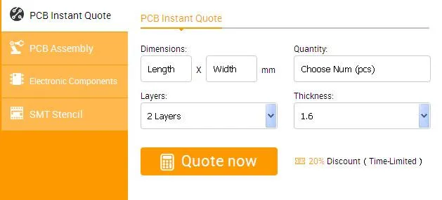
Start by creating a new account on the manufacturer's website or log in to an existing one. Ensure your contact and shipping information is accurate. - Upload Your Gerber Files
Upload your zipped Gerber files, which contain all the necessary PCB layout information. Most manufacturers support standard Gerber RS-274X format. Double check to ensure all the required files are included. - Specify PCB Parameters
Specify essential parameters such as the number of layers, board dimensions, material (e.g., FR4), thickness, copper weight, surface finish (e.g., HASL, ENIG), solder mask color, and silkscreen color. Be sure to follow the manufacturer's guidelines for each parameter. - Upload Bill of Materials (BOM) and Component Placement Files
If you require assembly services, upload your BOM, which lists all the components needed for your board, and component placement files. Make sure each item in the BOM matches the part number and required specification. - Select Quantity
Enter the number of PCBs you need. This may impact pricing. Verify the pricing updates when selecting the quantity. - Review and Confirm Order
Carefully review all parameters, files, quantities and pricing before proceeding to the next step. Double check for any inaccuracies. - Add to Cart and Checkout
Add your order to the cart and proceed to checkout. Select your preferred shipping method and enter your payment information. - Place the Order
After successfully submitting payment, you will receive an order confirmation and tracking information. Save this confirmation for your records.
Many manufacturers offer online platforms with real-time quotation and DFM (Design for Manufacturability) checks. Utilizing these features can greatly streamline the ordering process and reduce potential errors. Some manufacturers may also offer specialized services or materials, which can be chosen during the order process. Be aware that certain choices may affect pricing or lead times.
Understanding Lead Times and Shipping When You Order Custom PCB
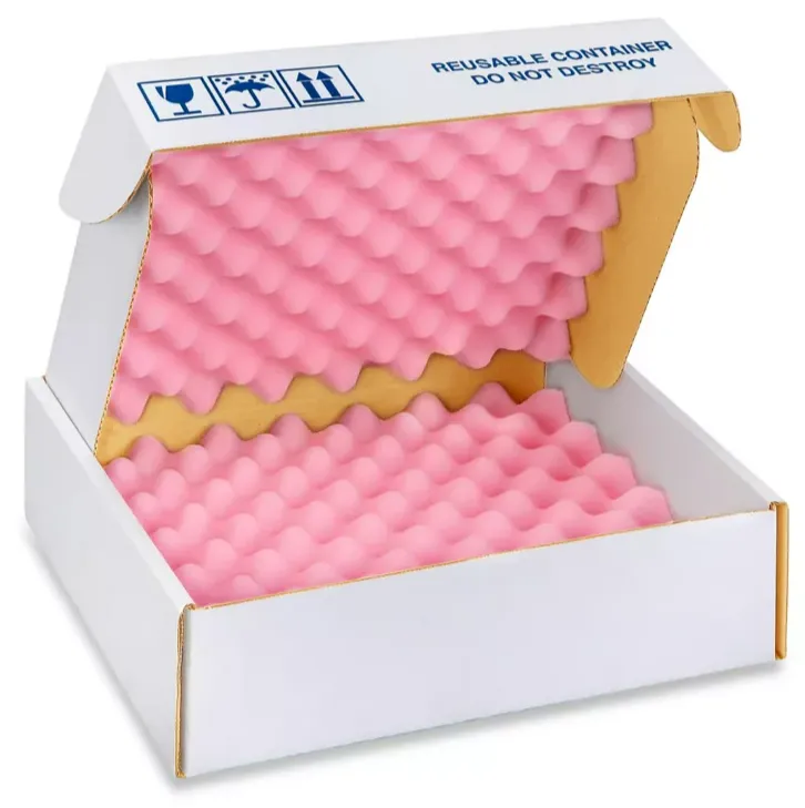
Lead time and shipping are crucial considerations when you order custom PCBs, impacting project timelines significantly. Understanding these factors allows for better planning and avoids potential delays. Lead time refers to the time it takes for the manufacturer to produce your PCBs, while shipping time is the duration required for the boards to reach you.
| Factor | Impact on Lead Time | Impact on Shipping Time |
|---|---|---|
| PCB Complexity (layers, features) | Longer production time for complex designs due to intricate fabrication processes | Minimal impact |
| Order Volume | Larger orders can increase lead times due to production scheduling and resource allocation. | Larger orders may require more time for handling, packaging and potentially slower shipping options. |
| Manufacturer's Current Workload | High demand can lead to extended lead times as the manufacturer processes existing orders. | Minimal impact |
| Material Availability | Shortages or delays in obtaining specific materials can extend production time. | Minimal impact |
| Shipping Method | Minimal impact | Shipping method (e.g., express, standard) dramatically affects delivery time. |
| Destination | Minimal impact | Distance to the delivery location will influence the overall delivery duration. |
| Customs and Import Procedures | Minimal impact | International shipments may face delays due to customs inspections and clearance. |
Factors such as PCB complexity, order volume, and the manufacturer's current workload directly affect lead times. Additionally, the type of shipping service selected, as well as distance and custom processes, significantly affect delivery time. To minimize delays, always confirm lead and shipping times with your chosen manufacturer before placing your order and choose the fastest shipping method for time-sensitive projects.
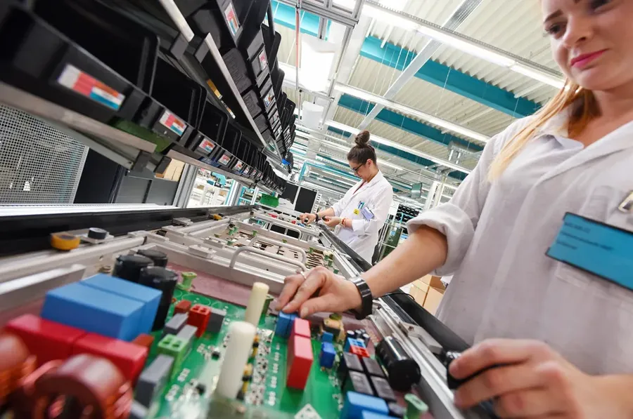
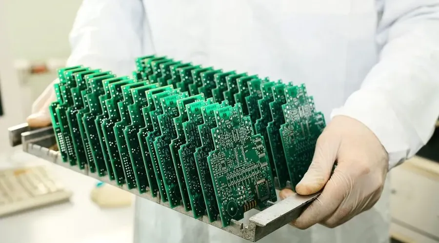
Quality Control and Inspection After You Order Custom PCB
Upon receiving your custom PCBs, a thorough quality control and inspection process is crucial to ensure they meet your design specifications and performance requirements. This step is not merely about finding flaws; it's about verifying the integrity of the manufacturing process and the reliability of your boards.
- Visual Inspection
Examine the PCB surface for any visible defects such as scratches, dents, or misalignments of layers. Check the solder mask for uniform coverage and proper alignment with pads. Inspect silkscreen printing for legibility and accuracy. Pay close attention to the edges for burrs or uneven cutting. - Dimensional Accuracy
Verify that the board dimensions match your specifications using precise measurement tools like calipers. Check the positions of mounting holes and cutouts. Ensure that the board thickness and layer stack-up meet the designed values. Any dimensional inaccuracies can impact proper fit within your final product. - Solder Pad and Via Inspection
Inspect solder pads for proper size, shape, and alignment. Ensure that all vias are correctly plated and that there are no broken or missing vias, which can impact electrical connections. Use magnification for a detailed inspection, as small defects in pads or vias can cause issues during component placement and soldering. - Connectivity Test
Use a multimeter or automated testing equipment to verify the electrical connectivity of your design. Check for shorts between traces and opens where connections should be. Perform continuity tests on each network to ensure all nets are properly routed and interconnected. This test is vital to avoid operational errors due to board flaws. - Layer Alignment Check
If your PCB has multiple layers, check the layer alignment using a microscope or specialized inspection equipment. Misalignment between layers can affect connectivity and overall performance. Verify the proper registration of each layer by carefully examining test points or via stacks. - Material Quality Check
If specific materials were required, such as high-Tg FR-4 or a special substrate, verify the material used matches the specification. Material composition directly affects performance, reliability, and thermal properties.
Troubleshooting Common Issues When You Order Custom PCB
Encountering issues with custom PCBs after ordering is not uncommon, but knowing how to address them efficiently is crucial. This section provides a guide to identifying common problems and the appropriate steps to resolve them, including when and how to contact your manufacturer effectively.
- Identifying Common PCB Issues
Typical problems include dimensional inaccuracies, layer misalignments, short circuits, open circuits, solder mask defects, and component placement errors. Thorough visual inspection using magnification is often the first step in identifying problems. - Dimensional Inaccuracies
Verify board dimensions using calipers against your design specifications. Discrepancies could indicate a manufacturing deviation. If found, notify the manufacturer immediately to understand the potential cause and to evaluate the usability of the boards for your needs. - Layer Misalignment
Misalignment between layers can lead to functional issues. Examine the board using magnification to see if vias and pads on different layers align correctly. If misalignment is observed, contact your manufacturer, as this usually indicates a process flaw in the PCB production. - Short Circuits and Open Circuits
Test for shorts using a multimeter to ensure there are no unintended connections between traces and pads. Check for open circuits that might interrupt intended paths. If discovered, consult your design to ensure the design is not the cause, as a manufacturing error or issue in the Gerber files may be the problem. Contact the manufacturer promptly if the issue stems from the manufacturing process. - Solder Mask Defects
Examine the solder mask for inconsistencies, such as partial coverage or mask presence on pads where it should be absent. Such issues can impede solderability and affect reliability of solder joints. If these issues arise, notify the manufacturer immediately. - Component Placement Errors
Check to ensure that components are placed in the correct orientation and location with respect to pads and other board components. These errors may be due to inaccurate BOM or pick-and-place data. Component placement issues need to be corrected, as they can prevent proper functionality of the final assembly. - Contacting the Manufacturer Effectively
Provide comprehensive details of the issue, including photographic evidence, specific location of defects, batch number of your boards and any testing data. Clear, concise and comprehensive data provided to the manufacturer will enable them to efficiently analyze the problem and identify a solution. Ensure you are familiar with your manufacturer’s specific contact channels (email, phone, or ticketing system). - Following Manufacturer's Guidelines
Your manufacturer will likely have a specific procedure for reporting errors. Following these guidelines ensures timely processing and resolutions. Include all requested information for a smooth issue resolution process, such as providing all error details, batch information, and your purchase order number. - Documentation
Keep records of the problem, communication with manufacturer, as well as any potential resolutions. This documentation can be critical in case further action is needed.
Frequently Asked Questions About Ordering Custom PCBs
This section addresses common inquiries regarding the custom PCB ordering process, providing detailed answers to guide you through each step. Understanding these FAQs can help streamline your experience and ensure you receive PCBs that meet your exact specifications.
- What are Gerber files, and why are they necessary when I order custom PCB?
Gerber files are the standard file format used in the PCB manufacturing industry. They contain all the essential information about your PCB design, such as copper layers, solder mask, silkscreen, and drill locations. Manufacturers use these files to fabricate your board precisely. Without accurate Gerber files, your PCB may not be produced correctly, or not at all. - What does the layer count of a PCB mean when I order a custom PCB?
The layer count refers to the number of conductive copper layers within your PCB. A single-layer PCB has one copper layer, a double-layer PCB has two, and multi-layer PCBs can have more. Each layer is separated by a non-conductive substrate. The number of layers you need will depend on the complexity of your circuit. More complex circuits typically require more layers to route all of the necessary connections. - How can I ensure my PCB design is manufacturable before I order a custom PCB?
To ensure manufacturability, adhere to Design for Manufacturing (DFM) guidelines. These guidelines include minimum trace widths, spacing, hole sizes, and annular ring dimensions for vias. Use PCB design software that includes DFM checks. Consider performing a DFM review with your chosen manufacturer before finalizing your order to avoid unnecessary delays and issues. - What factors influence the cost of ordering a custom PCB?
Several factors impact PCB costs, including the size and complexity of the board, the number of layers, materials used (such as FR-4, aluminum, or ceramic), the quantity ordered, and the chosen manufacturer. Special processes like impedance control, blind vias, and specific surface finishes also contribute to the overall price. Requesting a detailed quote from manufacturers can help you understand these cost drivers. - How do I choose the right PCB manufacturer for ordering my custom PCB?
Consider several factors when selecting a manufacturer: capabilities (minimum trace width/spacing, layer count), material offerings, price, turnaround time, customer reviews, and quality certifications (like ISO). Consider requesting samples from a few manufacturers to evaluate their quality before placing a large order. Also, evaluate their support responsiveness and ability to address questions promptly. - What are the usual lead times when I order custom PCBs, and what can affect them?
Lead times for PCB production vary depending on the manufacturer and complexity of the order. Standard lead times may range from a few days to several weeks. Factors such as the complexity of the PCB design, the number of boards in the order, the manufacturer's workload, and any extra processes can influence lead times. Expedited services are available from some manufacturers but often come with a higher cost. - What quality control steps should I consider after I order custom PCBs and receive them?
Upon receiving your PCBs, conduct a visual inspection to check for any defects such as scratches, misalignments, or incorrect silkscreening. Use a multimeter to check for shorts, open circuits and trace continuity. If you have specialized test equipment, you can test the impedance, and signal integrity. Confirm that the board thickness, dimensions and material matches what you requested, by comparing it with the manufacturer's specifications.
Ordering custom PCBs doesn't need to be confusing. By following the steps outlined in this article, and taking the time to compare all options before you order custom pcb, you can ensure a successful and cost-effective manufacturing process, allowing you to focus more on creating and building cutting-edge electronic products. Always ensure the design and technical specifications are complete to avoid any delays.