Navigating the World of PCBs with Way PCB: A Comprehensive Guide
Printed Circuit Boards (PCBs) are the unsung heroes of modern electronics, silently powering everything from smartphones to industrial machinery. In the vast landscape of PCB manufacturers, navigating the best options and understanding the nuances can feel daunting. This article serves as your comprehensive guide to understanding the role of Way PCB in this ecosystem, delving into what makes a reliable PCB partner and how they can meet your diverse needs. We will explore key considerations in PCB design, fabrication, and assembly, ultimately empowering you to make informed decisions for your projects.
Understanding the Basics of PCBs
Printed Circuit Boards (PCBs) are the foundational building blocks of nearly all modern electronic devices. Serving as the structural base and electrical pathway, PCBs mechanically support electronic components while providing the conductive traces needed to interconnect them. These boards are meticulously designed to ensure the correct functionality and performance of electronic systems.
PCBs are essential for enabling miniaturization, reliability, and mass production of electronic devices. They replace the tedious and error-prone process of hand-wiring, allowing for complex circuits to be efficiently produced and integrated into various applications.
| PCB Type | Description | Typical Applications |
|---|---|---|
| Single-Sided PCBs | Components are mounted on one side, with conductive traces on the other. Simplest and least expensive. | Simple electronics, toys, and basic control circuits. |
| Double-Sided PCBs | Components and conductive traces are present on both sides of the board, increasing circuit density. | Intermediate complexity electronics, power supplies, and industrial controls. |
| Multilayer PCBs | Consist of three or more layers of conductive traces separated by insulating material, enabling very complex designs. | High-performance electronics, computers, and advanced communication systems. |
Way PCB: A Profile
Way PCB is a prominent printed circuit board (PCB) manufacturer, distinguished by its comprehensive suite of services, specialized expertise, and advanced technological capabilities. They cater to a diverse clientele, ranging from individual hobbyists to large-scale industrial clients, offering solutions tailored to various PCB requirements.
Way PCB's core services span the entire PCB lifecycle, encompassing design assistance, fabrication, and assembly. Their facilities are equipped with state-of-the-art machinery, enabling them to produce high-quality PCBs with precision and efficiency.
A key specialization of Way PCB is in the manufacturing of complex multilayer PCBs, crucial for sophisticated electronics. They also offer expertise in specialized PCB materials, including FR-4, aluminum-backed, and flexible PCBs, catering to different application demands. The integration of advanced technologies in their manufacturing process ensures they can meet strict industry standards, such as IPC Class 2 and Class 3.
| Service Area | Description |
|---|---|
| PCB Fabrication | Manufacturing of bare PCBs from single-sided to complex multi-layer boards using advanced etching, drilling, and plating techniques. |
| PCB Assembly | Component sourcing, placement, soldering, and testing services using automated SMT lines, suitable for both small batch prototypes and large-scale production. |
| Design Support | Offering DFM (Design for Manufacturability) review, schematic review, and Gerber file review to ensure optimal PCB designs that are efficient and cost-effective. |
| Material Expertise | Proficiency in working with various materials, including standard FR-4, aluminum-backed PCBs for better thermal management, and flexible PCBs for dynamic applications. |
| Technological Capabilities | Utilizing advanced machinery including laser direct imaging, automated optical inspection (AOI), and impedance testing, ensuring high levels of precision and quality control. |
Key Considerations in PCB Design
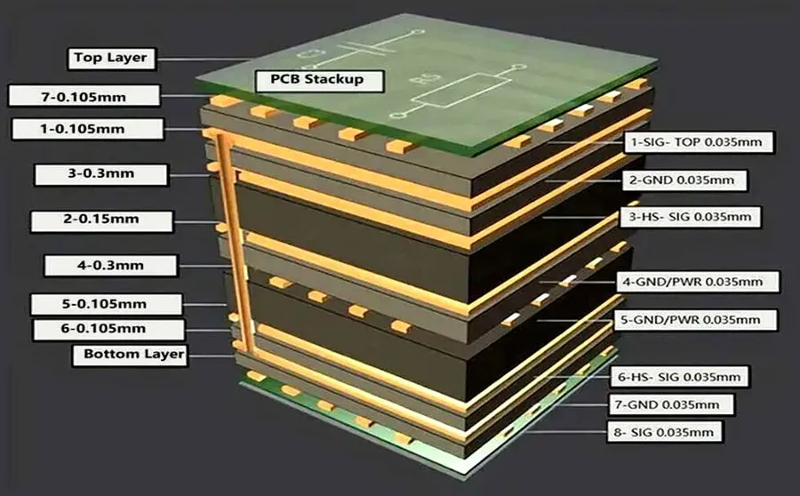
Effective PCB design hinges on a multitude of interconnected parameters, each critical to the final performance and reliability of the electronic product. These parameters include layer stack-up, trace routing, component placement, and thermal management, all of which require careful consideration and adherence to best practices.
| Design Parameter | Description | Best Practice Considerations |
|---|---|---|
| Layer Stack-Up | Arrangement of conductive and insulating layers within the PCB. | Balance signal integrity with cost; consider impedance control, power and ground planes, and signal layers. For high speed designs, plan the stack up early in the process. |
| Trace Routing | Pathways for electrical signals connecting components. | Minimize trace length, avoid sharp bends, and maintain consistent impedance. Ensure adequate spacing to prevent signal interference (crosstalk). High-speed signals should be routed with consideration for characteristic impedance. |
| Component Placement | Strategic positioning of components on the PCB. | Group related components together; consider thermal characteristics to prevent hotspots. Optimize for efficient assembly, reduce trace length, and balance component distribution. Allow space for test points and thermal reliefs. |
| Thermal Management | Dissipation of heat generated by components. | Employ thermal vias, heat sinks, and proper component placement; ensure adequate airflow and use of thermally conductive materials. Account for the thermal resistance of materials and plan for thermal reliefs near components that dissipate significant amounts of heat. |
These design parameters should not be viewed in isolation; rather, they interact with each other. For example, an inappropriate layer stack-up can negatively affect trace impedance and cause signal integrity issues. Similarly, improper component placement can lead to thermal management problems. A holistic design approach that considers these parameters collectively is essential for creating high-performing, reliable PCBs.
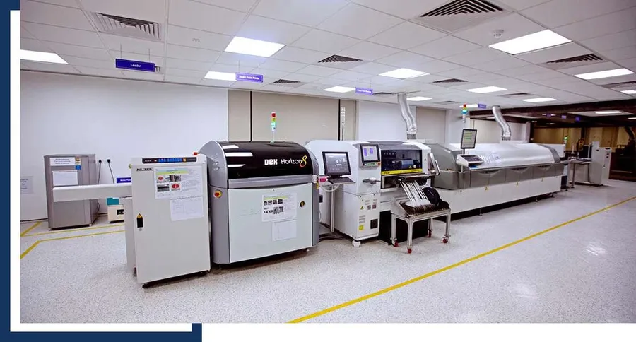
The PCB Manufacturing Process with Way PCB
The fabrication of Printed Circuit Boards (PCBs) at Way PCB involves a complex series of precise steps, transforming raw materials into the functional platforms for electronic circuits. This process integrates advanced techniques and stringent quality controls to ensure the delivery of reliable and high-performance PCBs.
- Material Selection
The process begins with the selection of appropriate base materials, typically FR-4 (Flame Retardant 4), known for its balance of cost, mechanical strength, and electrical insulation properties. Other materials, such as aluminum or specialized laminates, are chosen based on application-specific requirements like thermal management or high-frequency performance. - Circuit Design Transfer
The design data, generated using Electronic Design Automation (EDA) software, is converted into a format suitable for manufacturing. This involves creating a set of photolithographic masks representing the conductive traces, pads, and other circuit elements on each layer of the PCB. - Inner Layer Imaging and Etching
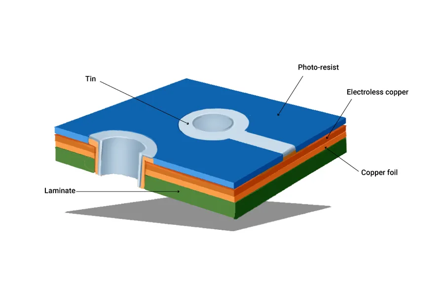
For multilayer PCBs, the inner layers undergo imaging, where a photosensitive resist is applied and exposed to UV light through the masks. This process defines the conductive patterns. The resist is developed, and the exposed copper is etched away using a chemical process, leaving the desired circuit traces. After etching, the resist is stripped, and the layers undergo an Automated Optical Inspection (AOI) to ensure quality. - Layer Lamination
The individual inner layers, along with prepreg (a bonding material), are stacked and laminated under high temperature and pressure. This process fuses the layers together, creating a solid substrate that is the multilayer PCB structure. Alignment is a critical aspect of this step, using precise mechanical tooling. - Drilling
Holes for component leads, vias (interlayer connections), and mounting are precisely drilled using Computer Numerical Control (CNC) drilling machines. The accuracy of this step is vital for proper component insertion and electrical connectivity. Drill sizes are carefully controlled to meet design specifications. - Electroless Plating
A thin layer of copper is deposited on the surface and hole walls through an electroless plating process. This conductive layer is essential for subsequent electroplating and establishing electrical contact through the vias. - Outer Layer Imaging and Etching
Similar to the inner layer process, the outer layers are imaged, developed and etched to define the final conductive patterns. This is followed by another AOI to check for defects, ensuring no shorts or opens on the outer layer. - Electroplating
Copper is electroplated onto the board, increasing the thickness of the traces and vias to meet current carrying requirements and to create a robust and conductive layer for solderability. - Solder Mask Application
A solder mask is applied to the PCB to protect the traces from corrosion and prevent solder bridging during component assembly. This layer is also imaged and developed to expose the areas for soldering, and it's often coloured (usually green), and acts as an insulator, and can reduce contamination. - Surface Finish
The exposed copper pads are then given a surface finish, such as HASL (Hot Air Solder Leveling), ENIG (Electroless Nickel Immersion Gold), or OSP (Organic Solderability Preservative), to protect the copper and ensure solderability. The specific finish is chosen based on the application and component type. - Silkscreen Printing
Silkscreen printing is the process of placing identification markings, component outlines, and company logos using a non-conductive ink. This layer provides important designators and helps in the assembly process. - Final Inspection and Testing
The finished PCBs are subjected to a final inspection and electrical testing including net list and continuity checks. This step ensures the functionality of the circuits, including shorts and opens, before the PCBs are packaged and shipped to the customer.
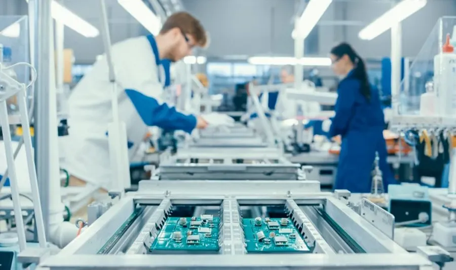
PCB Assembly Services at Way PCB
Way PCB provides comprehensive PCB assembly services, encompassing the entire process from component sourcing to final testing. This service is designed to transform bare PCBs into fully functional electronic assemblies, adhering to stringent quality control measures.
- Component Sourcing
Way PCB manages the acquisition of all necessary components, leveraging their established supply chain to ensure authenticity and quality. This includes passive components, integrated circuits, and electromechanical devices. - Component Placement
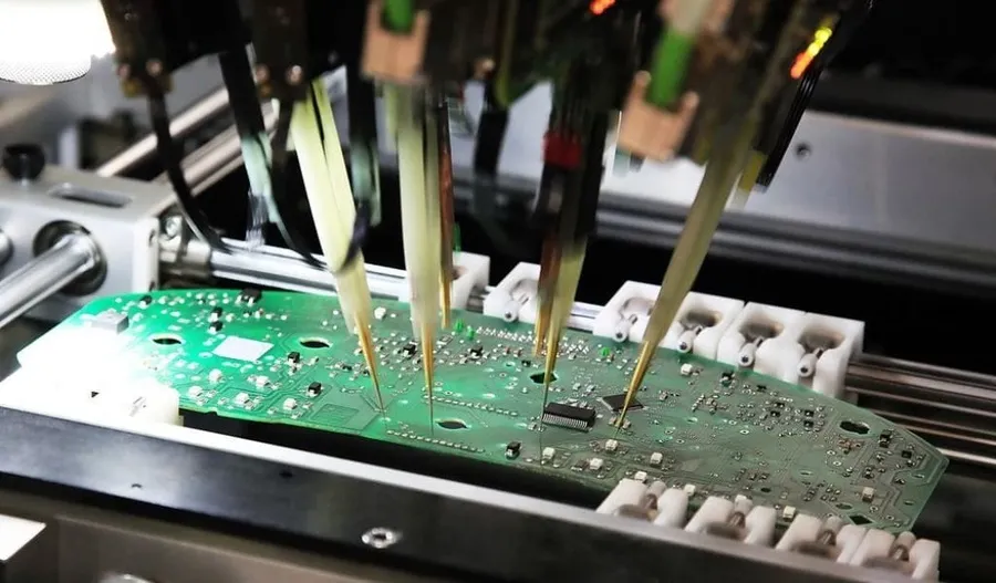
Using automated pick-and-place machines, components are precisely positioned onto the PCB according to the design specifications. This automated approach minimizes errors and improves production speed. - Soldering
Way PCB employs advanced soldering techniques such as reflow soldering for surface mount components and wave soldering for through-hole components. Soldering processes are carefully monitored to achieve robust and reliable electrical connections. - Inspection and Testing
Following the soldering process, each assembly undergoes rigorous inspection and testing. This may include visual inspection, automated optical inspection (AOI), in-circuit testing (ICT), and functional testing to verify performance and identify any defects. The quality control process ensures high reliability of the finished products.
| Service | Description | Way PCB's Approach |
|---|---|---|
| Component Sourcing | Procurement of electronic parts for assembly | Utilizes a vetted supply chain, including direct sourcing to reduce counterfeits and ensure the components meet customer specifications. |
| Placement | Precision mounting of components onto the PCB | Employs high-speed, high-accuracy pick-and-place machines, optimized for various component sizes and types. |
| Soldering | Creation of electrical connections between components and the PCB | Offers multiple soldering techniques (reflow, wave), tailored to the requirements of each assembly and component type. |
| Inspection & Testing | Rigorous checks on the completed assemblies to guarantee functionality | Incorporates AOI, ICT, and functional testing to ensure that all electronic products are operating as designed. |
Cost-Effective PCB Solutions with Way PCB
Achieving cost-effective PCB solutions with Way PCB requires a strategic approach that considers design optimization, material selection, and production process efficiency. By carefully analyzing these factors, significant cost reductions can be achieved without compromising the quality or performance of the final product.
Several factors influence the overall cost of PCB manufacturing. Understanding these elements allows designers and engineers to make informed decisions that directly impact expenses:
- Material Selection
The type of material, such as FR-4, high-frequency laminates, or flexible substrates, significantly affects cost. Standard materials like FR-4 are generally more cost-effective than specialized alternatives. - Layer Count
The number of layers in a PCB directly impacts manufacturing complexity and cost. Single-sided and double-sided boards are cheaper than multi-layer designs. - Board Size and Dimensions
Larger boards require more material and processing, which increases cost. Optimizing board size to minimize waste is crucial. - Trace Width and Spacing
Extremely fine traces and small spacing necessitate more precise manufacturing processes, thereby raising costs. Adhering to standard design rules can reduce complexity and costs. - Hole Sizes and Plating
The number and size of drilled holes, especially microvias, can add to the manufacturing expenses, as they require precise and time-consuming processes. The amount of plating also influences cost. - Surface Finish
Different surface finishes (e.g., HASL, ENIG, Immersion Tin) come with varying costs. Selecting the most appropriate finish for the application can help reduce expenses. - Order Volume
Larger production volumes typically result in lower per-unit costs, as fixed setup and tooling expenses are spread across more units.
To achieve cost optimization, consider the following strategies:
- Design for Manufacturability (DFM)
Implementing DFM principles early in the design phase can significantly reduce manufacturing costs. This includes avoiding overly complex designs and adhering to standard design rules. - Standard Component Selection
Choosing readily available and standard components instead of specialized ones can lower component costs and simplify the assembly process. - Panelization Optimization
Panelizing multiple PCBs on a single panel can reduce material waste and overall production costs, especially for high-volume manufacturing. Carefully optimizing the panel layout to maximize space efficiency is essential. - Efficient Layer Stack-Up
Carefully choose the number of layers needed for signal routing and ensure that each layer is necessary. Avoid adding unnecessary layers, as each layer adds to manufacturing complexity and cost. - Thorough Design Review
A rigorous design review before manufacturing can catch errors and avoid expensive rework or scrap. - Negotiate Pricing with Way PCB
Discuss your project requirements and production volume with Way PCB to explore potential discounts and cost-saving opportunities. Establishing a good relationship with the manufacturer can lead to more favorable pricing.
| Cost Optimization Strategy | Description | Impact on Cost |
|---|---|---|
| DFM | Designing with manufacturing capabilities in mind. | Reduces rework, lowers scrap, reduces production time, and increases yield. |
| Material Optimization | Selecting materials appropriate for the application. | Reduces material cost. |
| Component Selection | Using standard and readily available components | Lowers component acquisition cost and shortens lead times. |
| Panelization | Panelizing multiple PCBs together | Lowers material waste and production time. |
| Layer Stack-Up Optimization | Using only the needed layers for signal routing | Lowers production costs. |
| Design Review | Thorough verification of the design before manufacturing | Avoids rework and scrap by catching potential issues early. |
Frequently Asked Questions About Way PCB Services
This section addresses common queries about Way PCB, providing clear and concise answers to help users better understand their services and offerings. We aim to provide practical insights into the most frequently asked questions regarding their PCB manufacturing and assembly processes.
- What services does Way PCB offer?
Way PCB provides comprehensive PCB manufacturing services, including fabrication, assembly, and component sourcing. They specialize in producing high-quality PCBs ranging from simple single-layer boards to complex multilayer designs, along with offering various assembly options including SMT and through-hole. - When should vias be used in PCB design?
Vias are crucial when you need to connect traces on different layers of a multi-layer PCB. They are essential for routing signals effectively, managing thermal paths, and optimizing space utilization within your circuit design. The choice of via type (e.g., through-hole, blind, buried) depends on factors like layer count, signal integrity requirements, and cost. - What are the key factors to consider when choosing a PCB manufacturer?
When selecting a PCB manufacturer, key factors include the manufacturer's quality standards and certifications, turnaround time, cost, customer support responsiveness, technology capabilities (e.g., minimum trace width and spacing), and material options. It's crucial to evaluate a manufacturer's experience with your specific project complexity and material needs. - What is FR-4 material and why is it commonly used by PCBWay?
FR-4 is a glass-reinforced epoxy laminate material widely used in PCB manufacturing because of its excellent electrical insulation, mechanical strength, thermal resistance, and cost-effectiveness. Its versatility and balance of properties make it a standard choice for many applications. Way PCB utilizes FR-4 due to its reliability and broad applicability. - How can I get a quote for PCB fabrication and assembly at Way PCB?
To obtain a quote from Way PCB, you generally need to submit your PCB design files (Gerber files) and a Bill of Materials (BOM) through their website. Providing detailed specifications, including layer count, material type, board dimensions, quantity needed, and assembly requirements, will ensure a precise and accurate cost estimate. - What file formats are accepted for submitting PCB designs to Way PCB?
Way PCB primarily accepts Gerber files (RS-274X format), which are the industry standard for PCB fabrication. Additionally, they may accept other formats such as Eagle, Altium, or KiCad files, though Gerber files are the most universally compatible for PCB manufacturing processes. - What are some common mistakes to avoid when designing a PCB for manufacturing with Way PCB?
Common errors include forgetting to include necessary clearances and design rules, choosing incorrect via sizes, failing to specify material and layer stack-up accurately, and not doing design rule checks. Ensuring that you adhere to Way PCB's specifications can help prevent costly errors during the fabrication process and result in a successful outcome.
Choosing the Right PCB Partner: Why Way PCB
Selecting the ideal PCB manufacturing partner is crucial for project success, and Way PCB distinguishes itself through a commitment to quality, reliability, and comprehensive customer service. This section delves into the key factors that set Way PCB apart in a competitive market, providing clear guidelines for making informed decisions.
Here's a breakdown of why Way PCB stands out:
- Commitment to Quality
Way PCB adheres to stringent quality control measures throughout the entire manufacturing process, from material selection to final inspection. This dedication ensures that each PCB meets or exceeds industry standards and client specifications. - Unwavering Reliability
Reliability is paramount in PCB manufacturing. Way PCB utilizes robust manufacturing processes and high-quality materials, which translate into consistent product performance and dependability. Their ability to deliver on time and as expected minimizes project delays and disruptions. - Comprehensive Customer Service
Way PCB prioritizes customer satisfaction through responsive and knowledgeable support. Their customer service team provides guidance throughout the project lifecycle, from initial design consultation to post-delivery support, ensuring a smooth and efficient experience. - Technological Capabilities
Way PCB is equipped with advanced manufacturing technologies, enabling them to produce a wide range of PCBs, from simple single-sided boards to complex multilayer designs. Their technological edge ensures they can accommodate diverse project requirements. - Competitive Pricing
While maintaining high quality, Way PCB also provides competitive pricing structures, making their services accessible to a wide range of clients from hobbyists to large enterprises. They aim to offer cost-effective solutions without sacrificing quality or performance.
| Factor | Way PCB Advantage | Competitive Comparison |
|---|---|---|
| Quality Control | Strict adherence to industry standards and rigorous inspections | Varies across manufacturers, some lacking detailed processes |
| Reliability | Consistent production and on-time delivery | Inconsistent, with some delays and defects |
| Customer Service | Dedicated support team and responsive communication | Often limited and not always responsive |
| Technology | Advanced equipment capable of handling diverse PCB designs | May lag with older equipment |
| Pricing | Cost-effective solutions without sacrificing quality | Ranges widely, some lack transparency |
Practical Tips for Successful PCB Projects with Way PCB
Achieving successful PCB projects with Way PCB requires a meticulous approach encompassing design verification, clear communication, and thorough testing. These practical tips are designed to minimize errors, ensure product functionality, and optimize the manufacturing process.
- Design Verification
Prior to manufacturing, conduct comprehensive design rule checks (DRC) and simulations to catch potential issues early on. These include, but are not limited to, trace width and spacing, component clearances, and thermal considerations. Utilizing design software's built-in tools for DRC is essential. Always double-check Gerber files and BOM (Bill of Materials) for accuracy. - Effective Communication
Maintain clear and consistent communication with Way PCB. Provide comprehensive design documentation, including detailed specifications, clear instructions, and any specific requirements. Be proactive in addressing questions or concerns from their engineering team, and ensure that all revisions are clearly documented and communicated to avoid misunderstandings. Confirm that Way PCB has the latest version of design files before production commences. - Proper Testing Procedures
Develop a robust testing plan and implement testing procedures to verify the functionality of your fabricated PCBs. Start with visual inspections to identify any surface defects. Utilize automated testing equipment for thorough electrical testing such as continuity, impedance, and signal integrity testing. Employ a test fixture suited for your design. Conduct functional testing of populated boards to ensure proper operation in the intended application. - Component Selection
Choose components that are readily available and that meet the design requirements of your PCB, with lead times and potential obsolescence taken into consideration. Check component datasheets carefully for electrical specifications and ensure that they are within the acceptable operating limits of your design. - Prototype First
Before committing to a large production run, manufacture a small number of prototypes to validate the design and identify any unforeseen issues. Testing prototypes under realistic conditions can reveal potential problems before large-scale production. This step can save time and money by addressing any design or manufacturing issues. - Utilize Way PCB’s Resources
Take advantage of Way PCB’s technical support and design for manufacturability (DFM) checks. Their expertise can identify potential design flaws or manufacturing issues that may have been overlooked. Use the tools that are offered to ensure your designs are optimised for the production process.
Understanding the nuances of PCB manufacturing and assembly is essential for any electronics project. Way PCB offers a comprehensive suite of services, from design to final assembly, and by understanding the processes involved, you can ensure the success of your project. This article aimed to provide clear guidelines, practical advice, and an in-depth understanding of how Way PCB can be an integral part of your electronic design journey, ensuring a path from idea to final product using the right PCB partner.