Order Custom PCBs Online: A Comprehensive Guide for 2024
In today's fast-paced world of electronics, custom printed circuit boards (PCBs) are essential for bringing innovative ideas to life. Whether you're a hobbyist, a student, or a professional engineer, the ability to order custom PCBs online is a game-changer. This guide will walk you through the process, showcasing the best options, comparing services, and providing insights to make ordering custom PCBs online as easy and efficient as possible, enabling you to quickly realize your electronic designs. Let's dive in!
Understanding Your PCB Needs Before Ordering
Prior to initiating an online order for custom Printed Circuit Boards (PCBs), a thorough evaluation of project-specific requirements is crucial. This involves defining precise parameters such as the PCB's dimensions, the number of conductive layers, the types of materials, and the total quantity needed. These pre-ordering considerations will ensure the fabricated PCBs are perfectly suited for your design, guide your selection of the appropriate manufacturer, and help to minimize the risk of costly design revisions.
- PCB Dimensions
Accurately measure the required length and width of your PCB. Consider the overall space your project allows, and any size constraints of your enclosure. - Layer Count
Determine the number of conductive layers needed for your circuit. More complex designs may require multiple layers for routing and signal integrity. Common options include single-layer, double-layer, and multi-layer PCBs. - Material Selection
Choose the appropriate base material for your PCB. Common choices include FR-4 (a versatile and cost-effective material), aluminum (for heat dissipation), and polyimide (for flexible circuits). Material selection will depend on temperature, electrical, and mechanical requirements. - Quantity of PCBs
Decide on the number of boards needed for prototyping, testing, or final production. Ordering in bulk can reduce per-unit costs but requires accurate demand forecasting. - Copper Thickness
Determine the required copper thickness for your design. Higher current applications might require thicker copper. - Surface Finish
Choose an appropriate surface finish to ensure good solderability and environmental protection of the pads. Common surface finishes include HASL, ENIG, and OSP.
Choosing the Right Online PCB Manufacturer
Selecting the appropriate online PCB manufacturer is crucial for the success of any electronics project. The ideal manufacturer will not only meet your technical specifications but will also align with your budget and timeline. A thorough comparison of different manufacturers is essential to ensure you obtain high-quality PCBs that are delivered on time and within budget.
When assessing potential manufacturers, consider their capabilities across various factors:
- Manufacturing Capabilities
This includes the number of layers they can produce, minimum trace width and spacing, and the types of materials they offer. Ensure these meet your project requirements. - Pricing Structure
Understand how the manufacturer calculates costs. Factors like board size, layer count, material, and quantity significantly influence the final price. Get quotes for both prototype and full production runs. - Lead Times
Compare the time it takes from design submission to delivery. Lead times vary based on manufacturing complexity and order volume, so choose a manufacturer that aligns with your project schedule. - Customer Service
Responsive and knowledgeable customer service can make a big difference, particularly if you encounter issues during the process. Check for multiple support channels, including email, chat, and phone. - Quality Control
Assess the quality control measures employed by the manufacturer, including inspections and testing procedures, to ensure that the final PCB meets your specifications. - Special Features
Determine if the manufacturer offers any special feature that may be useful, for example, impedance control, blind and buried vias, and surface finish options.
Some popular online PCB manufacturers include:
- JLCPCB
Known for its low-cost prototypes and quick turnaround times, suitable for smaller projects and hobbyists. - PCBWay
Offers a wide range of services and materials, suitable for both prototyping and production runs. - DigiKey
Primarily known as a component distributor but offers PCB manufacturing services, especially useful when ordering components and PCBs together.
The Ordering Process Step-by-Step
Ordering custom PCBs online involves a systematic process, beginning with the preparation of your design files and culminating in the delivery of your manufactured boards. This section provides a detailed walkthrough, ensuring clarity and efficiency at each stage. Successfully navigating each step is crucial for achieving accurate fabrication results.
- Preparing Your Gerber Files
The Gerber file is the industry standard for PCB manufacturing. Ensure your design software generates the correct Gerber files, including copper layers, solder mask, silkscreen, drill files, and any other required layers. Double-check these files for accuracy and completeness. - Selecting Board Parameters
Specify key parameters such as board dimensions, number of layers, material type (e.g., FR-4), copper thickness, and surface finish. Precise specifications at this stage are vital for the correct fabrication of your boards. - Uploading and Reviewing Your Design
Once the board parameters are defined, upload the Gerber files to the manufacturer's platform. Some manufacturers provide online viewers that allow you to visually inspect your board layout before proceeding. Review this preview carefully to identify any potential errors. - Obtaining a Quote
Based on your design and specifications, the online platform will generate a quote detailing the cost of fabrication. Compare quotes from different manufacturers, considering the balance between price and quality of the final product. - Placing and Confirming Your Order
After reviewing and accepting the quote, submit your order. Provide necessary contact and payment information. It is crucial to verify every detail of your order at this stage. This includes quantity, material, finish, and delivery address, to prevent any unexpected issues. - Payment Processing
Choose your preferred payment method and complete the transaction. Ensure you receive a confirmation of your payment and order. Most manufacturers will provide an order number that can be used to track your order status. - Production and Shipping
After your payment, the manufacturer proceeds to produce your PCBs. Lead times may vary depending on the manufacturer and the complexity of your design. Once fabrication is complete, the manufacturer will ship your PCBs. They may provide tracking information so that you can monitor the shipping process.
Design Considerations for Successful PCB Fabrication
Successful PCB fabrication hinges on adhering to sound design practices that ensure manufacturability. This section details critical design considerations, including trace width and spacing, via placement, and compliance with Design for Manufacturability (DFM) guidelines, which will help prevent costly errors and ensure a functional final product.
- Trace Width and Spacing
Trace width and spacing are fundamental to PCB design. Trace width must be adequate to carry the intended current without overheating, and spacing must be sufficient to prevent shorts or arcing, especially for high-voltage applications. Standard trace width and spacing guidelines are often provided by manufacturers and should be strictly adhered to, varying with layer and application. - Via Placement
Vias are crucial for connecting layers of a multilayer PCB. Proper via placement is essential to ensure that signal integrity is maintained, and that the vias can be reliably manufactured. Keep vias away from sensitive areas and maintain sufficient clearance from other features. - Design for Manufacturability (DFM)
DFM guidelines ensure that the designed PCB can be reliably and cost-effectively fabricated. These guidelines include considerations like minimum hole sizes, solder mask clearances, and component placement rules. Following DFM from the outset will minimize errors and speed up production. - Component Clearance
Ensure sufficient clearance around components and between components for assembly, soldering, and testing. This includes proper spacing between components and the board edges or other features to facilitate easy component placement and rework. - Pad Design
Pad design is critical for reliable soldering. The shape, size, and spacing of pads must correspond to component footprints and must be optimized for the soldering process (e.g., reflow or wave soldering). Poor pad design can lead to soldering defects and poor electrical connections. - Copper Pour and Thermal Relief
Copper pours on PCBs serve to enhance signal integrity and thermal management. When adding copper fills, it is essential to include appropriate thermal relief for component pads, which allows heat to dissipate evenly during soldering, preventing issues such as tombstoning, a defect where a component stands on end rather than sitting flat on the board.
By strictly adhering to these design guidelines, you can mitigate the risk of manufacturing defects and ensure the smooth fabrication and optimal performance of your PCBs. Consult the specific design rules provided by your chosen manufacturer to address particular process constraints.
Cost Factors for Custom PCB Orders
Understanding the cost drivers when ordering custom PCBs online is crucial for effective budget management. Several factors influence the final price, including material selection, board dimensions, layer count, and turnaround time. A comprehensive understanding of these variables empowers informed decision-making and cost optimization.
| Cost Factor | Impact on Cost | Considerations |
|---|---|---|
| Material Selection | Significant | FR-4 is standard; advanced materials increase cost. |
| Board Size | Directly Proportional | Larger boards require more material and processing. |
| Layer Count | Significant | More layers require more complex manufacturing. |
| Lead Time | Inversely Proportional | Express services increase cost. |
| Quantity | Economies of Scale | Per-unit cost decreases with larger production runs. |
| Surface Finish | Moderate | ENIG (Electroless Nickel Immersion Gold) is more expensive than HASL (Hot Air Solder Leveling). |
| Special Features | Variable | Controlled impedance, blind/buried vias, and other advanced features increase cost. |
Quality Control and Assurance

Ensuring the quality of custom PCBs is paramount to the success of any electronic project. Rigorous quality control and assurance processes during PCB fabrication are crucial for verifying the reliability and functionality of the boards, involving both visual and electrical testing to meet stringent specifications.
- Visual Inspection
A thorough visual inspection is the first step in quality control, where technicians examine PCBs for physical defects. This includes checking for any misalignment of layers, broken or missing traces, incorrect solder mask application, and issues with the silkscreen. High magnification is often used to identify even the smallest flaws, ensuring the board meets dimensional and cosmetic standards. This process is critical for preventing mechanical issues and ensuring proper component placement. - Electrical Testing
Electrical testing is essential to verify the proper functionality of the PCB. This testing commonly includes open/short tests to confirm that there are no unintended connections or breaks in the circuitry. More advanced tests, such as Flying Probe and Bed of Nails testing, may be utilized to check complex boards, verifying that every electrical connection is correctly formed and that there is no impedance or resistance outside of design specifications. This helps to prevent functionality issues in the finished product. - Automated Optical Inspection (AOI)
Automated Optical Inspection (AOI) is a method that uses high-resolution cameras and sophisticated software to identify defects on PCBs with speed and accuracy. AOI systems can detect issues that might be missed by visual inspection such as small shorts, opens, or incorrect solder paste deposits. AOI ensures consistent quality across mass-produced boards. - X-Ray Inspection
For multi-layered PCBs with internal components, X-Ray inspection is a vital method to verify the integrity of vias and through-hole plating. It can also be used to examine solder joints and ball grid array (BGA) connections that are not visible through conventional means, ensuring that connections are structurally sound and free of voids. - Functional Testing
Functional testing simulates the working conditions of the PCB, assessing its performance when it is fully populated with components. This type of test verifies whether the manufactured PCB performs as intended within the specific application, verifying the assembled board works as intended and detects any issues related to components or fabrication that were missed in previous testing.
Frequently Asked Questions About Ordering Custom PCBs Online
This section addresses common questions regarding ordering custom PCBs online, providing clear, concise answers to streamline the process. These FAQs will cover essential aspects such as file formats, turnaround times, payment methods, and shipping options.
- What file formats are required to order custom PCBs online?
The primary file format required is Gerber, which encapsulates all the necessary layers and design information for PCB fabrication. Additionally, many manufacturers accept drill files (Excellon format) and BOM (Bill of Materials) files for assembly services. Ensure all files are exported correctly according to the manufacturer's specifications. Some may also accept ODB++. - How long does it typically take to receive custom PCBs after ordering online?
Turnaround times vary considerably based on the manufacturer, complexity of the PCB, and selected shipping method. Prototype orders can range from 24 hours to a week, whereas production runs can take several weeks. Always verify with the manufacturer for an accurate lead time and consider potential delays due to shipping and customs. - What payment methods are commonly accepted for online custom PCB orders?
Most online PCB manufacturers accept common payment methods such as credit cards (Visa, MasterCard, American Express), PayPal, and bank transfers. Some may offer payment options in multiple currencies. Verify your desired payment method is available before placing your order. - Do manufacturers offer international shipping for custom PCB orders placed online?
Yes, most online PCB manufacturers offer international shipping. Shipping options and costs vary based on the delivery destination. Be aware of customs duties and taxes, as the recipient is often responsible for such charges. Always review the shipping terms to avoid surprises. - Can I get a quote for my custom PCB order before placing it?
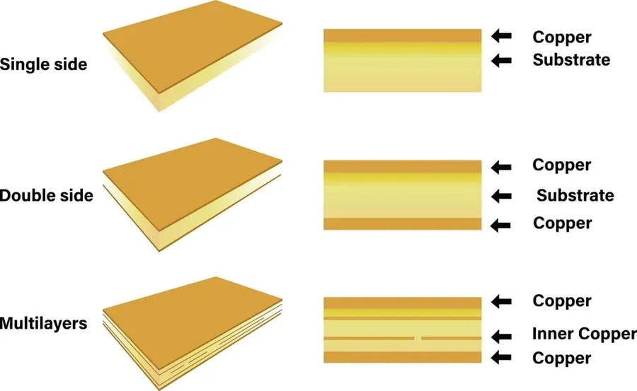
Yes, most online manufacturers offer an instant quote system where you can upload your Gerber files and board specifications to get an estimate. This helps you determine the cost before placing the order. Some manufacturers may also provide manual quotes for complex designs. - What does the term 'PCB Layer' mean in relation to my custom board order?
A PCB layer refers to a single conductive copper layer on a printed circuit board. Typical PCBs can be single-sided, double-sided, or multi-layered, with the latter ranging from 4 to 30+ layers. The complexity of your circuit and routing requirements will determine the necessary layer count. - What are common issues that might cause errors in manufacturing when ordering custom PCBs?
Several design or file issues can result in manufacturing errors. These include insufficient trace width/spacing, unplated or improperly designed vias, incorrect drill files, unclear board outline definition, and lack of adherence to Design for Manufacturing (DFM) rules. Thoroughly review and adhere to the manufacturer's guidelines to prevent such issues.
Comparing PCB Manufacturers: A Detailed Analysis
Selecting the right PCB manufacturer is crucial for the success of your project. This section provides a detailed comparative analysis of popular PCB manufacturers, focusing on key factors such as pricing, lead times, material options, and user reviews, enabling you to make an informed decision when you order custom PCB online.
| Manufacturer | Price (Prototype) | Lead Time (Prototype) | Material Options | User Reviews | Strengths | Weaknesses |
|---|---|---|---|---|---|---|
| JLCPCB | Very Competitive | Fast (2-5 Days) | FR-4, Aluminum | Generally Positive | Low cost, fast turnaround, large customer base, good for hobbyists | Limited advanced material and technology, occasional quality issues reported |
| PCBWay | Competitive | Moderate (3-7 Days) | FR-4, Aluminum, Flexible | Positive | Wide range of materials, good customer support, various advanced options | Slightly more expensive than JLCPCB for simple PCBs, lead times a bit longer |
| AllPCB | Competitive | Moderate (3-7 Days) | FR-4, Aluminum | Mixed | Good variety of services including PCBA, user friendly platform, can handle bigger volumes | Customer support issues, quality control sometimes inconsistent |
| Seeed Fusion | Moderate | Moderate (3-7 Days) | FR-4, Aluminum, Flexible | Positive | Easy to integrate with their platform, good for smaller to midsize projects, responsive support | Higher cost compared to other budget options, complex orders can be costly |
| OSH Park | Premium | Moderate (7-12 Days) | FR-4 | Very Positive | High quality boards, great for complex prototypes, good customer support, community friendly | More expensive for single orders, longer turnaround times, limited options |
| DigiKey | Higher | Variable | Multiple Options | Positive | Wide range of options, high quality, good support and reputable supplier, extensive catalogue of electronic parts | More expensive, complex online quoting system |
Tips for a Smooth Online PCB Ordering Experience
Ordering custom PCBs online can be streamlined for efficiency and accuracy by paying close attention to detail and maintaining clear communication throughout the process. The following tips will help ensure a successful outcome when ordering custom printed circuit boards online.
- Double-Check Your Design Files
Before uploading your Gerber files, meticulously review them for any errors or omissions. Verify that all layers are correctly aligned, drill files are accurate, and the silkscreen and solder mask layers are as expected. Use a Gerber viewer to ensure that the generated files accurately represent your intended design. This critical step can prevent costly errors and delays in the manufacturing process. - Choose the Correct PCB Parameters
Carefully select the correct parameters for your PCB, including material type (e.g., FR-4, aluminum), board thickness, copper weight, and surface finish. Incorrect selections can lead to fabrication issues. Check with the manufacturer if you are unsure of the best options for your application. - Clearly Communicate with Your Manufacturer
Maintain open and clear communication with your chosen PCB manufacturer. Ask clarifying questions about their capabilities, and be available to respond promptly to their questions and potential issues. Effective communication can prevent misinterpretations, saving time and resources and is particularly important for complex designs. Include detailed comments on each layer. - Plan for Lead Times
Be realistic about production and shipping times. Factor in the lead time quoted by the manufacturer, and add an extra buffer for unexpected delays. Starting the ordering process with adequate time before your required delivery date minimizes stress and keeps your project on schedule. Consider potential delays due to holidays or high order volumes. - Use a Reliable Shipping Method
Select a reputable shipping carrier that can offer tracking and insurance. The shipment process is an important part of the overall process, so choosing a good shipping method will greatly improve the ordering experience, especially if your order is time sensitive or has high value. - Prepare Comprehensive Documentation
Provide detailed documentation along with your Gerber files, including specifications for any unique or non-standard features, materials, and tolerances. Include assembly notes if you plan to order PCB assembly as well. The clarity of documentation greatly helps avoid errors during fabrication. - Keep Records of all Transactions
Keep records of all your correspondence with the manufacturer, as well as transaction information, like order numbers and payment receipts. It makes it easier to refer back when clarifying any potential order issues. Maintaining a detailed record helps in resolving any disputes or questions effectively.
Ordering custom PCBs online has become essential for both rapid prototyping and large-scale production. By understanding the process, selecting the right manufacturer, and adhering to best practices in PCB design, you can ensure a seamless and efficient experience. Whether you're looking for a few prototype boards or a large production run, the right online vendor can provide the custom printed circuit boards you need with the speed and quality you expect, enabling you to order custom pcb online and bring your electronic project to reality. Always compare your options and take advantage of the various online tools to achieve the best possible results. Start today and see your electronics projects come to life.