Seamless PCB Prototyping: Design & Order Online
In today's rapidly evolving tech landscape, the ability to quickly prototype and order Printed Circuit Boards (PCBs) online has become indispensable. The fusion of accessible online design tools and efficient manufacturing services empowers both hobbyists and professional engineers to bring their electronic ideas to life. This article will navigate you through the process of online PCB design and order, exploring software options, reliable manufacturers, and key considerations to ensure your project's success.
Choosing the Right Online PCB Design Software
Selecting the appropriate online PCB design software is crucial for a successful project, influencing everything from initial schematic capture to the final Gerber file generation. This choice impacts efficiency, accuracy, and ultimately, the cost of your printed circuit board. An optimal software solution will provide a balance of user-friendliness, feature richness, and cost-effectiveness, aligning with the specific requirements of your design.
| Feature | EasyEDA | KiCad (Cloud Version) | Other Options |
|---|---|---|---|
| Ease of Use | Beginner-friendly interface, intuitive tools | Slightly steeper learning curve, powerful features | Varies significantly, needs evaluation based on specific software |
| Library Availability | Extensive user-generated and pre-built library, growing fast | Large community library, requires some management | Ranges from good to limited, needs careful investigation |
| Collaboration Capabilities | Built-in team collaboration features | Cloud version facilitates team work | Varies across platforms, some offering better collaboration than others. |
| Simulator Integrations | Basic simulator integrated | Can be used with external SPICE simulators | Some have simulator or links, others do not |
| Pricing | Free for basic use, paid options for advanced features | Free and open-source | Wide range, some free, some premium with recurring subscriptions |
The table above highlights key features to compare when choosing online PCB design software. Consider these elements in the context of project needs to make a well-informed decision.
Creating Your PCB Design Online
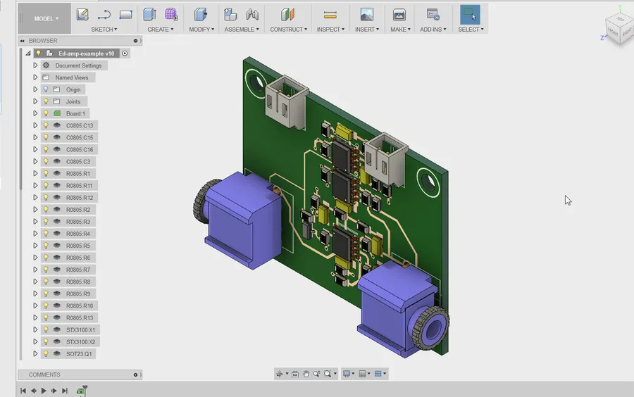
Creating a Printed Circuit Board (PCB) design online involves a structured process, typically encompassing schematic capture, component placement, routing, and the generation of manufacturing files, ensuring a design ready for production. This section details each of these critical phases.
- Schematic Capture
The initial step involves creating a schematic diagram that represents the electronic circuit. This process includes selecting components from the online library and connecting them using logical symbols to define circuit functionality. The schematic serves as the blueprint for the physical layout of the board. - Component Placement
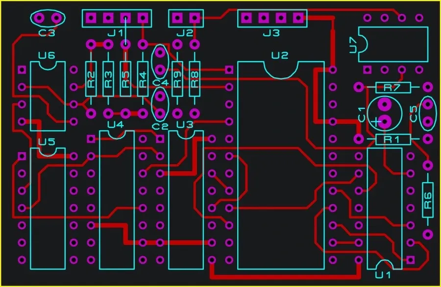
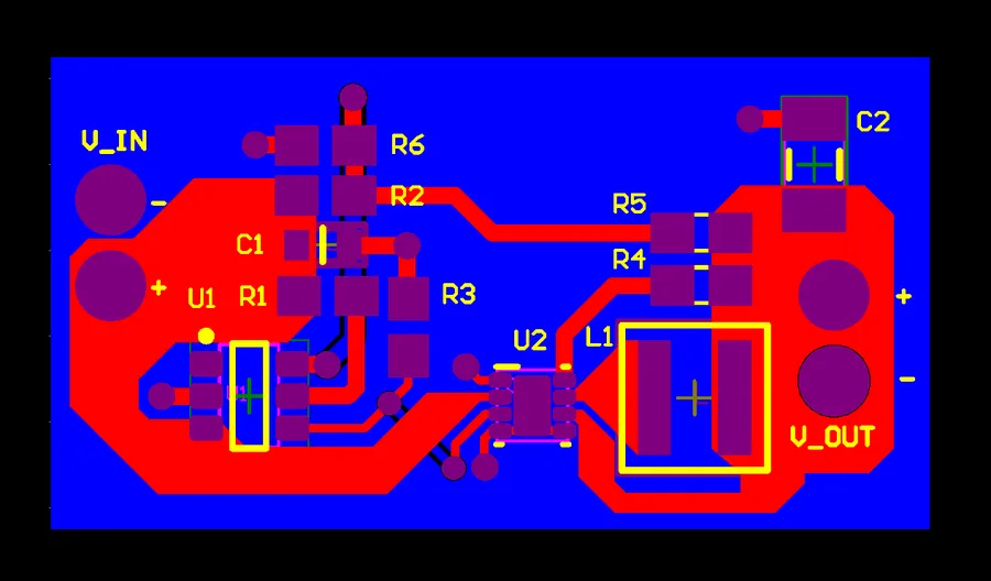
Once the schematic is complete, components are placed on the virtual PCB board. Consider the board's physical constraints, component sizes, heat dissipation, and electrical characteristics when deciding on placement. Effective placement can improve routing efficiency and board performance. - Routing
Routing involves establishing conductive pathways between components using copper traces on the PCB. This stage requires a careful approach, taking into account signal integrity, impedance control, and board layer limitations. Automated routing tools and manual adjustments are often used in this phase. - Generating Gerber Files
The final step is generating Gerber files. These files are the standard input for PCB fabrication, containing all the necessary information for the manufacturer to produce the physical board. This includes layer data, drill files, and component outlines. Ensure all design rule checks (DRC) pass and all files are correctly exported before order placement.
Preparing for Online PCB Order
Successfully ordering PCBs online hinges on meticulous preparation of your design files and a thorough understanding of manufacturer specifications. This stage ensures your online PCB design translates accurately into a physical product, minimizing delays and costly revisions. The key is to generate the correct Gerber files and drill files, and select the appropriate PCB material.
- Gerber File Generation
Gerber files are the industry standard for PCB manufacturing data. They represent each layer of your PCB design, including copper traces, pads, silkscreen, and solder mask. Ensure your design software's Gerber export settings are correct and generate all necessary layers. Common layers include: Top Copper, Bottom Copper, Solder Mask Top, Solder Mask Bottom, Silkscreen Top, Silkscreen Bottom, Drill File, and Board Outline. - Drill File Generation
The drill file specifies the locations and sizes of all drilled holes on your PCB. It's crucial to generate this file correctly, selecting the appropriate units (usually inches or millimeters) and format (Excellon format is common). Verify that all required holes for vias, component leads, and mounting points are accurately represented. - Manufacturer's Specifications
Each PCB manufacturer has unique design specifications that you need to follow precisely. These typically include minimum trace width, minimum spacing between traces, minimum hole sizes, and other design constraints. Carefully review the specifications from your chosen manufacturer *before* starting the design process to prevent issues with fabrication. Deviations from these specifications can cause delays or require costly design iterations. - Design Rules Check (DRC)
Always perform a comprehensive design rules check (DRC) within your PCB design software before ordering. This process automatically verifies that your design complies with the manufacturer's specifications and highlights any violations. Addressing these violations prior to submission will help prevent manufacturing errors. - PCB Material Selection
The choice of PCB material significantly impacts the performance and cost of your PCB. FR-4 is a common material and is suitable for a wide range of applications, but you may need to choose other materials based on your design requirements, such as for high-frequency or high-temperature applications. This material selection must be made before you order your PCB.
Selecting a Reliable Online PCB Manufacturer

Choosing the right online PCB manufacturer is crucial for a successful prototyping and production process. This selection directly impacts the quality, cost, and delivery timeline of your printed circuit boards. Key considerations include manufacturing capabilities, pricing, customer service, and the overall ordering experience.
Several online PCB manufacturers have established themselves as industry leaders, each with its own strengths and specialties. Understanding the nuances of these providers will empower you to make an informed decision aligning with your project's unique requirements. Below, we explore critical factors to consider.
| Manufacturer | Layer Count | Min. Track/Space | Material Options | Lead Time | Price | Specialization |
|---|---|---|---|---|---|---|
| JLCPCB | 1-16 layers (prototyping), up to 32 (mass production) | 4mil | FR-4 standard, Aluminum, Rogers, etc. | 2-5 days (prototyping), 1-3 weeks (mass production) | Very competitive, especially for prototypes | High-volume, low-cost PCBs |
| PCBWay | 1-16 layers (prototyping), up to 40 (mass production) | 4mil | FR-4, Aluminum, Flexible, Rogers etc. | 3-7 days (prototyping), 1-4 weeks (mass production) | Competitive pricing across services | Complex PCB assembly, diverse range of materials |
| DigiKey | Up to 16 layers | 4mil | FR-4, Polyimide | Varies, usually 1-3 weeks | Higher prices for low volumes | Wide array of electronic components and other services |
| AllPCB | 1-32 layers | 3mil | FR-4, Aluminum, Rogers | 3-7 days | Competitive | High-layer count PCBs, fast turnaround |
| Seeed Studio Fusion | 1-16 layers | 4mil | FR-4 standard, Aluminum, Rogers, etc. | 3-7 days | Competitive | Fast prototyping and small batch PCB fabrication |
Beyond these factors, consider the following before making your selection:
- Customer Reviews:
Assess customer feedback, focusing on the quality of the boards, responsiveness of customer support, and adherence to lead times. - Order Process:
Ensure the manufacturer has a streamlined order process that is easy to navigate and has sufficient documentation requirements. Verify that their systems support file uploads, BOM specification, and design review requirements. - Payment Options:
Verify that they support all available options such as Paypal, Credit card, or Bank transfers etc. - Shipping Considerations:
Evaluate shipping costs, delivery times, and the use of tracked shipping to allow full access to the shipping process. Ensure the manufacturer ships to your country.
Understanding PCB Manufacturing Options and Costs
The cost and performance of a Printed Circuit Board (PCB) are significantly influenced by the chosen manufacturing options. These options encompass a range of factors from material selection to finishing processes, each contributing to the final product's suitability for its intended application, this section explores these key elements in depth to better inform design and order decisions.
| Manufacturing Option | Description | Cost Impact |
|---|---|---|
| Surface Finish | Types include HASL (Hot Air Solder Leveling), ENIG (Electroless Nickel Immersion Gold), and Immersion Tin/Silver. Each offers varying levels of solderability, corrosion resistance, and cost. | ENIG generally more expensive than HASL; Immersion Tin/Silver provides good performance at a mid-range price. |
| Via Types | Through-hole vias, blind vias, and buried vias influence routing complexity, layer count and signal integrity. Blind and buried vias increase complexity but enhance design density and reduce routing space. | Blind and buried vias add cost due to increased manufacturing complexity. |
| Solder Mask Colors | Green is standard, but other colors are available (e.g., red, blue, black, white). While mostly aesthetic, specific colors can affect visual inspection and contrast. Choosing a non-standard color may increase cost. | Non-standard colors may lead to a slight increase in manufacturing costs. |
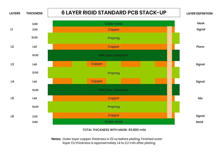
| Layer Stack Up | The number of layers in the PCB design influences impedance control, routing density, and overall performance. More layers increase the complexity and cost. | Increased layer count significantly increases manufacturing costs. |
| PCB Material | Materials like FR-4 (most common), Rogers (high-frequency applications), and aluminum (heat dissipation) impact performance, thermal management, and overall cost. | Rogers and aluminum substrates are more expensive than FR-4. |
| Panelization | Ordering multiple PCBs on a single panel, using a process called panelization, can reduce the cost per PCB by optimizing the use of manufacturing tools and materials | Panelization reduces unit cost but requires an initial panelization setup cost |
Several additional factors significantly impact the final PCB cost. Order volume plays a crucial role, with larger quantities typically resulting in lower unit prices. The complexity of the design, including the number of vias, component density, and trace width also directly affects manufacturing expenses. Furthermore, expedited manufacturing and shipping options can increase costs.
In conclusion, understanding the interplay between various manufacturing options and their cost implications is essential for making informed decisions during the online PCB design and order process. By carefully evaluating these factors, designers and engineers can optimize both the performance and cost of their PCBs, ensuring they meet the application's specific needs while staying within budget.
Essential Quality Control Checks for Online PCB Orders
Before finalizing your online PCB order, meticulous quality control checks are paramount to minimize errors and ensure a smooth manufacturing process. These checks encompass design rule compliance, accurate Gerber file generation, and bill of materials verification. Rigorous adherence to these steps reduces the likelihood of costly revisions and delays.
- Design Rule Check (DRC)
The Design Rule Check (DRC) is an automated process performed by PCB design software that verifies your layout conforms to the manufacturer’s specifications. Key checks include trace widths, clearances between traces and pads, via sizes and spacing, and drill hole sizes. Failing DRC checks can lead to manufacturing defects such as shorts or opens. Most PCB design platforms have built-in DRC functionality, which can be customized to match your specific manufacturer's rules. - Gerber File Verification
Gerber files are the standard file format used for PCB fabrication. Verification ensures that your Gerber files accurately represent your intended design. This involves using a Gerber viewer to inspect each layer (copper layers, silkscreen, solder mask, drill data). Specifically, look for errors in pad shapes, trace connections, text legibility, and layer alignment. Incorrect Gerber files can lead to misinterpretation of your design by manufacturers and a faulty board. - Bill of Materials (BOM) Accuracy
The Bill of Materials (BOM) is a list of all components required for your PCB assembly. Accuracy is essential to avoid delays in assembly or incorrect component placement. Ensure that each component part number, quantity, and description are accurate. Verify component footprints match the package on the BOM to prevent errors. Double check the BOM against your schematic, especially when using multiple vendors for component purchasing.
Frequently Asked Questions About Online PCB Design and Order
This section addresses frequently asked questions regarding online PCB design and ordering. We aim to clarify common concerns about file formats, turnaround times, minimum order quantities, payment security, shipping options, and software compatibility, ensuring a smoother process for both novice and experienced users.
- What file formats are required for online PCB ordering?
Most online PCB manufacturers require Gerber files (RS-274X format) which include copper layers, solder mask, silkscreen, and drill files. Some may also accept additional files like IPC-356 netlists for electrical testing or a Bill of Materials (BOM) for assembly services. Always check the manufacturer’s specific requirements before submitting your design. - How long does it typically take to receive my PCBs after ordering online?
Turnaround time varies significantly depending on the manufacturer, the complexity of the board, and the shipping method selected. Standard production can range from a few days to a couple of weeks. Expedited options are often available for an extra fee, providing quicker delivery. Check the lead times specified by your chosen manufacturer to make an informed decision. - What are the typical minimum order quantities (MOQs) for online PCB manufacturing?
Minimum order quantities vary among manufacturers. Some may offer single-piece prototyping options, while others may require a minimum of a few boards or panelized sets. The MOQs are usually driven by the manufacturing costs, setup time and material used, so understanding MOQs before design is crucial. Consider this factor in your cost calculations and choose a manufacturer accordingly. - How secure are online payment methods when ordering PCBs?
Reputable PCB manufacturers typically use secure payment gateways that utilize encryption to protect your financial information. Look for HTTPS protocols, padlock symbols and PCI DSS compliance to ensure your payment is processed securely. Credit card payments are common, and some manufacturers offer alternative payment methods such as PayPal. Always order from verified and secure websites. - What shipping options are typically available, and how are costs calculated?
Most online PCB manufacturers offer a variety of shipping methods, including standard postal services, express couriers, and sometimes freight shipping for large orders. Shipping costs vary depending on the weight, size, and destination of the package. Review different shipping options during checkout to determine the best balance between cost and delivery time. Customs and import duties may be applied and this is not included in the shipping fee. - Are there any compatibility issues between different PCB design software and online manufacturers' websites?
While Gerber file formats are mostly standardized, ensure your design software's settings for generating Gerber files match your manufacturer's requirements and specifications. Always review the manufacturer’s specific requirements, including file naming conventions, layer configurations, and units, which can vary. Check compatibility with the preferred file extension and run a design rule check using the manufacturer’s profile to avoid any misunderstandings, errors, and delays. - What should I do if I encounter an issue during the online ordering process?
Contact the manufacturer's customer support team for any issues you have. Many offer support through email, live chat, or phone, providing a range of options. Describe the issue with the most detail possible, including error messages and reference numbers to help the support team address the issue quickly and efficiently. Documenting issues and communication can be helpful in clarifying and correcting errors.
Tips for a Successful Online PCB Design and Order
Optimizing your online PCB design and order process is crucial for both first-time and experienced users to achieve high-quality results while minimizing errors and iterations. By paying close attention to common pitfalls and adopting best practices, you can significantly enhance the success rate of your PCB projects.
- Double-Check Your Design Rules
Before submitting your design, always run a thorough Design Rule Check (DRC) on your chosen online PCB design platform. This critical step helps identify violations such as trace width issues, clearances problems, and drill size errors that could lead to manufacturing defects. - Verify Gerber Files
After generating the Gerber files, use a free online Gerber viewer or the viewer provided by your chosen manufacturer to visually inspect each layer. Ensure that all traces, pads, and vias are correctly represented and that there are no unexpected artifacts or missing elements. This avoids unexpected problems and delays from the manufacturer side. - Accurate Bill of Materials (BOM)
Create and meticulously verify your BOM against your design. Include exact part numbers, manufacturer details, and quantities for each component. An incorrect BOM can result in delays and additional costs due to incorrect components being ordered or missing parts. - Choose the Right PCB Material and Surface Finish
Selecting the appropriate material and surface finish is vital for the functionality and lifespan of your PCB. Consider factors such as operating temperature, signal frequencies, and intended use environment. Consult with your manufacturer if you are unsure about these options. - Understand Manufacturing Specifications
Each online PCB manufacturer has unique specifications for board size, layer count, minimum trace width, and via sizes. Review these specifications carefully before starting your design to make sure your design can be manufactured as intended. Ignoring these requirements may lead to the design not being accepted. - Use Standard Library Components
Whenever possible, utilize standard library components within your online PCB design software. This reduces errors compared to creating custom footprints, which increases the risk of incorrect design. In cases of custom components, meticulously check the footprint for accuracy. - Plan for Panelization
For larger production runs, consider panelization to reduce manufacturing costs. Determine how many boards can be efficiently fitted onto a standard manufacturing panel and plan the design accordingly. Follow manufacturer guidelines for panel spacing and fiducial marks. - Communicate with Your Manufacturer
Don't hesitate to reach out to your manufacturer's support team if you encounter any issues or have questions about the manufacturing process. Clear communication helps prevent misunderstandings and ensures a smoother order process.
The process of online PCB design and order has become streamlined and accessible, making it possible for anyone to bring their electronic designs to life efficiently. By carefully selecting the right software, understanding manufacturing options, and adhering to recommended practices, you can create high-quality PCBs that meet your project needs. With services like those offered by JLCPCB and PCBWay, the ability to design and order PCBs online is now easier than ever, accelerating the development process and moving your project from concept to reality with speed and efficiency. Start your online pcb design and order journey today.