Understanding Electronic PCBs: From Basics to Advanced Applications
In today's technology-driven world, electronic devices are everywhere, and at the heart of nearly every gadget lies the unassuming printed circuit board (PCB). This essential component is the foundation upon which electronic circuits are built. This article delves into the details of electronic PCBs, from their basic definition and types to the intricate processes involved in design and manufacturing, highlighting their critical role in the electronic world and beyond.
What is an Electronic PCB?
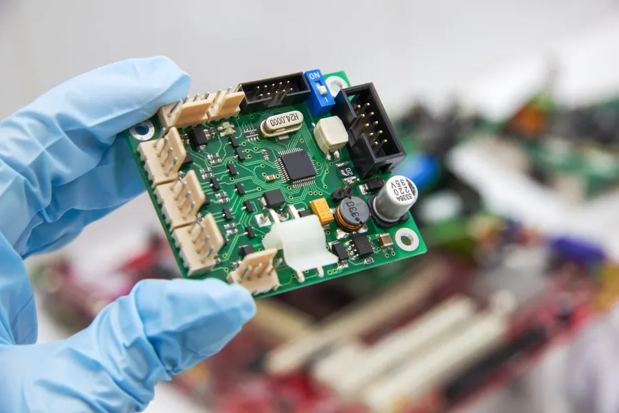
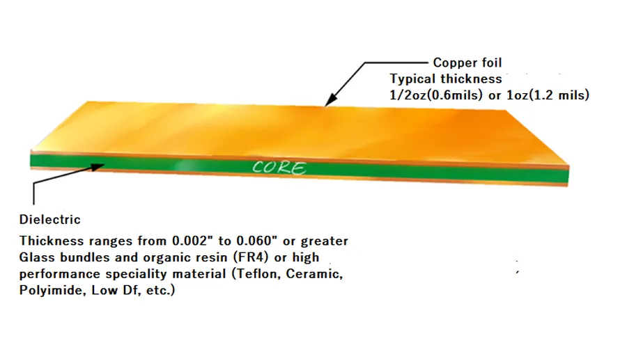
An electronic Printed Circuit Board (PCB) is the foundational element for nearly all modern electronic devices. It's a rigid or flexible base material, typically composed of fiberglass-reinforced epoxy (FR-4) or similar substances, upon which conductive pathways, known as traces or tracks, are etched from thin copper sheets. These traces act as electrical conduits, connecting electronic components and enabling the flow of electrical current to create functional circuits.
Key Components of an Electronic PCB
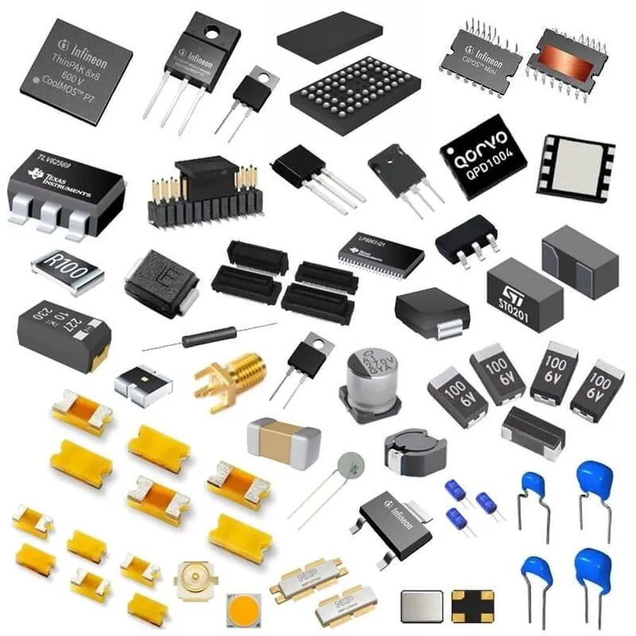
An electronic Printed Circuit Board (PCB) is more than just a foundation; it's a complex assembly of components working in harmony. Understanding these fundamental components—resistors, capacitors, inductors, and integrated circuits—is crucial to grasping how a PCB functions and underpins the operation of electronic devices.
| Component | Symbol | Function | Typical Applications |
|---|---|---|---|
| Resistors | Zig-zag line | Limit current flow, provide voltage drops | Voltage dividers, current limiting, pull-up/down resistors |
| Capacitors | Two parallel lines | Store electrical energy, filter signals | Power supply filtering, signal coupling, timing circuits |
| Inductors | Coil symbol | Store energy in magnetic field, filter signals, generate magnetic fields | Filtering, power conversion, RF circuits |
| Integrated Circuits (ICs) | Rectangular box with pins | Perform complex functions (logic, amplification, processing) | Microcontrollers, memory, op-amps, logic gates |
| Diodes | Triangle pointing to a line | Allow current flow in one direction, rectify AC | Rectification, signal detection, voltage regulation |
| Transistors | Multiple variations (BJT, FET) | Amplify and switch electronic signals and electrical power | Amplification, switching, voltage regulation |
Types of PCBs: A Comprehensive Overview
Printed circuit boards (PCBs) are not monolithic; they come in various configurations, each tailored to specific applications and complexities. Understanding the diverse types of PCBs—from single-sided to complex multi-layer boards—is crucial for selecting the appropriate technology for any electronic design. This section provides a comprehensive overview of the most common PCB types.
| PCB Type | Description | Layers | Typical Applications | Advantages | Disadvantages |
|---|---|---|---|---|---|
| Single-Sided PCB | Copper traces on one side of the substrate. Components are mounted on the other side. | 1 | Simple electronics, low-density circuits, toys | Cost-effective, simple to design and manufacture | Limited circuit complexity, lower component density |
| Double-Sided PCB | Copper traces on both sides of the substrate. Allows for more complex circuits. | 2 | Intermediate electronics, automotive, basic industrial equipment | Increased routing flexibility, higher component density than single-sided | More complex to manufacture than single-sided |
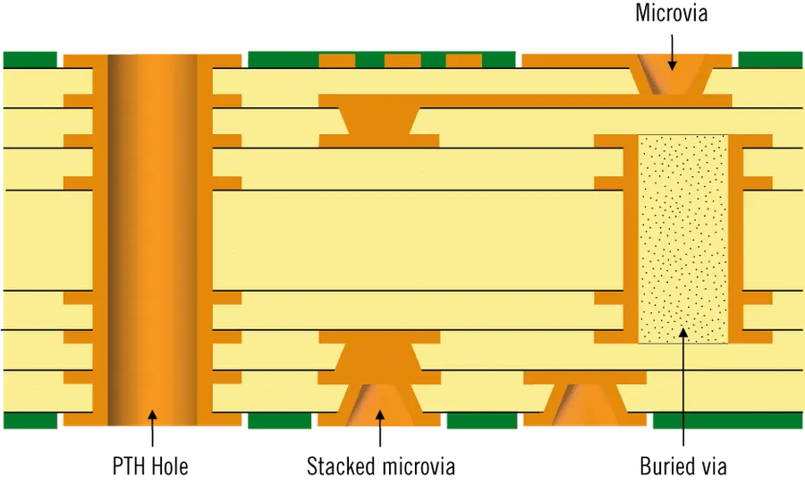
| Multi-Layer PCB | Three or more layers of copper traces separated by insulating layers. | 3+ | Complex electronics, computers, aerospace, high-speed devices | High component density, complex routing, supports impedance control | Expensive, more difficult to design and manufacture |
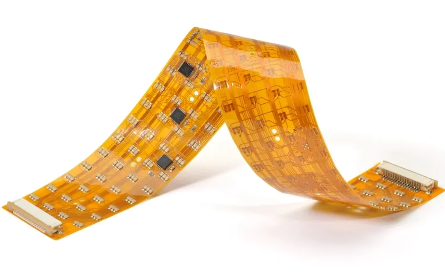
| Flexible PCB | Circuits built on a flexible substrate (e.g., polyimide). Can bend and fold. | 1-4+ | Wearable electronics, medical devices, automotive, aerospace, devices requiring bending or folding | Flexible, lightweight, reliable in harsh environments | More expensive than rigid PCBs, limited component mounting |
| Rigid-Flex PCB | Combination of rigid and flexible PCB sections. Offers mechanical flexibility and support. | 2+ | Aerospace, medical, and automotive applications, or any complex application that requires a combination of flexible and rigid boards. | Combines the flexibility of flex PCBs with the stability of rigid PCBs | Complex design and manufacturing, highest cost. |
The PCB Manufacturing Process: From Design to Reality

The fabrication of a Printed Circuit Board (PCB) is a complex, multi-stage process that transforms a digital design into a physical electronic component. This process demands precision at each step, utilizing a blend of chemical and mechanical techniques to ensure the final PCB meets the required specifications for electrical performance and reliability.
- Design and Schematic Capture
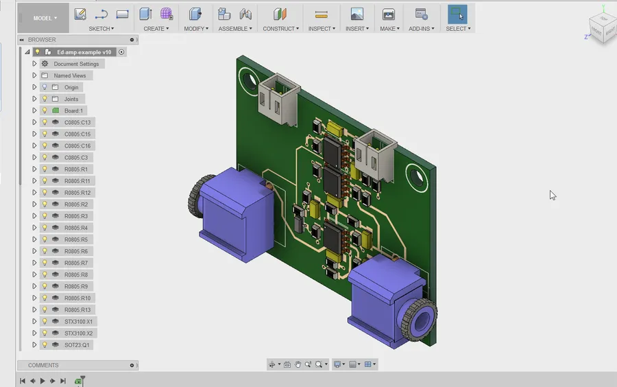
The process begins with the electronic design, capturing the circuit schematic using specialized software. This schematic represents the electronic components and their interconnections. Design rules checks are implemented to minimize downstream errors. - PCB Layout and Routing
The schematic is then translated into a physical layout, determining the placement of components and the routing of electrical traces. This involves meticulous planning to optimize signal integrity, minimize interference, and ensure efficient heat dissipation. Consideration of board dimensions, layer stack-up, and impedance control are essential. - Film Generation
Once the layout is complete, film is generated for each layer of the PCB. This film acts as a mask in subsequent steps and must be highly accurate to match the designed layout. - Copper Clad Lamination
The prepared substrate, usually FR-4 or another suitable material, is laminated with a thin layer of copper foil on one or both sides. The copper will form the conductive pathways of the circuit. Multilayer PCBs require multiple layers of this substrate and copper foil to be laminated together. - Etching
The exposed copper is then removed by a chemical process, leaving only the desired circuit traces as defined by the film mask. Etching requires controlled chemical baths and careful monitoring to ensure precise trace widths and spacing. - Drilling
Holes are drilled through the PCB to accommodate through-hole components and vias (interlayer connections). This process requires precision drilling machines to accurately place each hole according to design specifications. Automated drilling techniques are common. - Plating
After drilling, the holes are plated with a conductive material (usually copper), creating the vias. Plating ensures reliable electrical contact between layers. The surface of the PCB will also receive a surface finish (such as ENIG or HASL) for solderability and corrosion resistance. - Solder Mask Application
A solder mask is applied to the PCB to protect the traces from oxidation and prevent solder bridges during component assembly. The solder mask is typically a green epoxy-based ink, but other colors are available. - Silkscreen Printing
A silkscreen layer is added to the PCB, providing component reference designators and other information for assembly and testing. This step enhances the usability and maintainability of the assembled product. - Testing
The fabricated PCBs are subjected to electrical testing to verify that the circuits are working correctly and that there are no shorts or opens. Test methods can include flying probe tests, bed of nails tests or automated optical inspection. This step is crucial for ensuring that the PCB is functional and ready for component assembly. - Profiling & Final Inspection
The individual PCBs are profiled, which is the cutting process to produce the final shape of the board from larger manufacturing panels. Final inspection is undertaken for visual defects and dimensional accuracy to ensure that the PCBs are ready for use in the intended product.
PCB Design Essentials: Tools, Techniques, and Considerations
Effective PCB design is crucial for the functionality and reliability of electronic devices, encompassing schematic capture, layout, routing, and adherence to signal integrity, thermal management, and component placement best practices. This phase is not just about connecting components; it's about creating a robust, efficient, and manufacturable electronic system.
The process begins with schematic capture, a digital representation of the electronic circuit, created using specialized software. This schematic serves as the blueprint for the physical PCB layout. Following schematic capture, PCB layout involves physically arranging components and drawing conductive tracks (traces) to establish the electrical connections, and is an iterative process that requires careful consideration of various factors.
- Schematic Capture
Creating a digital representation of the electronic circuit using specialized software. It forms the blueprint for the PCB layout. - Component Placement
Strategic arrangement of electronic components on the board, considering size, thermal properties, and signal paths. Proper placement minimizes interference and optimizes signal integrity. - PCB Layout and Routing
Physically arranging components and creating the conductive pathways to establish electrical connections. Routing needs to minimize trace lengths, prevent crosstalk, and ensure manufacturability. - Signal Integrity Analysis
Analyzing the quality of electrical signals within the PCB. This involves considerations like impedance matching, reflections, and crosstalk. These are critical for high-speed signal paths and high-frequency circuits to prevent signal degradation and ensure reliable operation. - Thermal Management
Addressing the heat generated by electronic components during operation. This involves proper component selection, layout considerations (using heat sinks and thermal vias), and thermal analysis tools to ensure components operate within safe temperature limits. - Design Rule Checks (DRC)
Utilizing software tools to verify the design against a set of predefined rules. DRC ensures that the PCB is designed to meet specific manufacturing and performance standards.
| Design Consideration | Description | Importance |
|---|---|---|
| Component Placement | Strategic arrangement of components | Optimizes signal integrity, thermal performance, and manufacturability. |
| Signal Integrity | Ensuring signal quality through trace impedance control and minimal crosstalk | Critical for reliable high-speed and high-frequency operations. |
| Thermal Management | Dissipating heat effectively using heat sinks, thermal vias | Prevents overheating and premature component failure. |
| Layer Stack-up | Configuring the arrangement of copper and insulating layers | Manages impedance, provides ground planes, and optimizes power distribution. |
| Design Rules | Adhering to manufacturing constraints and industry standards | Ensures the PCB can be produced accurately and reliably. |
In summary, PCB design is a critical phase in product development that requires expertise in electronic engineering, materials science, and manufacturing processes. A well-designed PCB optimizes functionality, reliability, and cost-effectiveness of the final electronic product. The use of advanced software tools and rigorous design processes are crucial to achieve successful outcomes.
Materials Used in Electronic PCBs: From Substrate to Conductors
The performance and reliability of an electronic PCB are heavily dependent on the materials used in its construction. These materials range from the substrate that forms the base of the board to the conductive materials that carry electrical signals, and also include the protective layers and markings. The proper selection of these materials is critical for achieving the desired electrical, thermal, and mechanical characteristics.
| Material | Purpose | Typical Composition | Key Characteristics |
|---|---|---|---|
| Substrate (e.g., FR-4) | Provides mechanical support and electrical insulation. | Woven fiberglass cloth with epoxy resin. | High strength, good electrical insulation, flame retardant. |
| Copper | Forms conductive traces and pads. | High-purity copper. | Excellent electrical conductivity, solderability. |
| Solder Mask | Protects traces from oxidation and shorts during soldering. | Epoxy or acrylic based polymer with pigments. | Provides electrical insulation, heat resistance, solderability. |
| Silkscreen | Provides component labels and board identification. | Epoxy or acrylic-based inks. | Provides visual markings, good adhesion, durable. |
Beyond these core materials, other substances like plating materials (e.g., tin, gold) and adhesives also play a critical role in specific PCB functionalities. The careful selection and understanding of each of these materials are critical for ensuring high-quality and reliable electronic circuit board.
Frequently Asked Questions about Electronic PCBs
This section addresses common questions regarding electronic PCBs, providing clear and concise answers to enhance understanding and dispel misconceptions. These questions cover fundamental aspects of PCB technology, addressing typical user queries.
- What exactly is an electronic PCB (Printed Circuit Board)?
An electronic PCB is a foundational component in electronics, acting as a base material made of insulating substrate that has conductive pathways, known as traces, etched onto its surface. These traces are typically made of copper and provide electrical connections between various electronic components, facilitating the operation of circuits. PCBs serve as both a mechanical support and an electrical pathway for components. - What are the main types of electronic PCBs, and what distinguishes them?
Electronic PCBs come in various types, each suited for different applications. The main types include: Single-sided PCBs, which have conductive traces on one side only; Double-sided PCBs, with traces on both sides, allowing for more complex circuits; Multilayer PCBs, which are more complex with multiple layers of conductive material; Flexible PCBs, using flexible substrates; and Rigid-flex PCBs, which combine both rigid and flexible sections. These types are distinguished by the number of layers, flexibility, and thus, complexity and application. - Are all circuit boards considered to be PCBs?
While all PCBs are circuit boards, not all circuit boards are PCBs. The term 'circuit board' can encompass a broader range of substrates and wiring methods, including breadboards and perfboards. A PCB specifically refers to a board with pre-etched conductive traces, whereas other circuit boards may use different methods for creating connections. Therefore, PCBs are a specific type of circuit board. - Why are electronic PCBs often perceived as expensive?
The cost of PCBs is influenced by several factors. These include the complexity of the design (number of layers, trace density), material selection, production volume, manufacturing precision, and required testing. Smaller production runs typically have higher unit costs due to setup expenses, while complex designs demand advanced manufacturing techniques, leading to increased prices. The combination of these factors contributes to the overall cost of a PCB. - How can the costs associated with PCB production be optimized?
Optimizing PCB costs involves multiple strategies. Designers can reduce complexity by minimizing the number of layers and simplifying the layout. Choosing standard, readily available materials can decrease costs. Volume production often results in a reduced per-unit cost. Partnering with reliable PCB manufacturers, optimizing testing strategies, and standardizing the design process further helps in controlling costs without compromising quality or reliability. Therefore, attention to design and production factors can reduce expenses. - What is the significance of the substrate material used in PCBs?
The substrate material in PCBs is critical as it provides the base for the circuit and impacts electrical performance, thermal management, and mechanical integrity. Common materials like FR-4 offer a good balance of properties but may not suit all applications. Specialized materials with lower dielectric constants or better thermal conductivity are required for higher frequency or high-power applications. The choice of substrate directly affects reliability and performance of the PCB. - What role does copper play in electronic PCBs?
Copper is a primary conductor in PCBs because of its high electrical conductivity and low cost. It forms the conductive pathways or traces that connect components. Copper layer thickness and trace design parameters are important to ensure adequate current carrying capacity and desired signal integrity. Copper plating is also used in through-holes to make connections between different layers in multilayer boards. Copper is essential for the functionality and reliability of the board.
Future Trends and Innovations in PCB Technology
The printed circuit board (PCB) industry is undergoing rapid transformation, driven by the relentless pursuit of miniaturization, enhanced performance, and environmental sustainability. These advancements are not only pushing the boundaries of what's possible in electronics but are also shaping the future landscape of various industries.
- Miniaturization
Driven by the demand for smaller and more portable devices, PCB miniaturization is a key trend. This involves developing finer line widths and spacing, allowing for more complex circuitry to fit into smaller form factors. Advanced fabrication techniques such as Micro-Via and HDI (High Density Interconnect) technology are critical to achieving this. The use of chip-scale packaging (CSP) and system-in-package (SiP) technologies further supports miniaturization efforts, integrating multiple components into a single package which drastically reduces the PCB size. - Flexible and Stretchable PCBs
Flexible PCBs, using materials like polyimide, are becoming increasingly popular in applications requiring bending or flexing, such as wearable electronics, automotive electronics, and medical devices. Stretchable PCBs, a more advanced form, are designed to withstand higher degrees of deformation and are pivotal in innovative designs where adaptability to dynamic surfaces is essential. The integration of conductive inks and elastic substrates is integral to realizing stretchable and conformal electronics. - Eco-Friendly Materials and Manufacturing
The industry is moving towards more sustainable practices, including the use of eco-friendly materials such as bio-based resins and lead-free solder. Environmentally conscious manufacturing processes, which minimize waste and harmful emissions are also gaining traction. Furthermore, life cycle assessments are being increasingly adopted to evaluate the environmental impact of PCBs from cradle to grave, driving innovation in sustainable PCB development and end-of-life management. - Advanced Materials for High Frequency Applications
The need for higher data rates and frequencies are propelling research in low loss dielectric and high thermal conductive materials. Materials such as PTFE (Teflon), ceramics and advanced composites are gaining adoption in high frequency applications. These materials ensure signal integrity and efficient heat management which is critical for higher performing systems. - Embedded Components
Embedding components directly within the layers of a PCB is a key trend. This integration technique reduces the overall size of the board, improves thermal performance, and enhances reliability. Embedding passives and even small ICs within the substrate allows for more intricate designs and greater space utilization.
These trends point towards a future where PCBs are not only functional but also adaptable, sustainable and high performing. Continuous innovation in material science, fabrication technologies and design methods will be essential to realize these advances. This evolution will be essential for the creation of more powerful, compact, and environmentally responsible electronic devices.
Comparing PCB Types: A Quick Guide
This section provides a comparative analysis of single-sided, double-sided, and multi-layer PCBs, highlighting their key differences in applications, advantages, and limitations. This is essential for engineers and designers when selecting the appropriate PCB type for a specific project.
| Feature | Single-Sided PCB | Double-Sided PCB | Multi-Layer PCB |
|---|---|---|---|
| Number of Layers | One conductive layer | Two conductive layers | Three or more conductive layers |
| Complexity | Least complex | Moderately complex | Most complex |
| Density | Lowest component density | Medium component density | Highest component density |
| Cost | Least expensive | Moderately expensive | Most expensive |
| Applications | Simple consumer electronics, basic lighting, low-density circuits | Intermediate consumer electronics, power supplies, simple industrial controls | Advanced electronics, high-speed circuits, complex systems, aerospace, medical devices |
| Advantages | Simple design, easy to manufacture, lowest cost | Increased circuit density, allows for more complex routing, good balance of cost and functionality | Highest circuit density, allows for complex routing and high-speed signals, suitable for advanced applications |
| Limitations | Limited complexity, difficult to achieve high-density designs, routing limitations | Moderate complexity, limited to two layers for routing, may have signal integrity issues in high-speed applications | Most expensive, complex design and manufacturing, may require specialized equipment |
Electronic PCBs are the backbone of nearly every electronic device we use today. From simple household appliances to sophisticated medical equipment, the electronic PCB ensures that components connect, communicate, and perform their intended functions reliably. Understanding the intricate world of PCBs, including their design, manufacturing processes, and the materials involved, is critical for anyone involved in the electronics industry. With continual innovation and emerging technologies, electronic PCBs will continue to evolve, enabling even more advanced capabilities and solutions across various fields.