Unlocking the Power of PCB: Design, Manufacturing, and Applications
From the smartphone in your pocket to the complex systems powering our cities, Printed Circuit Boards (PCBs) are the unsung heroes of modern technology. This article dives deep into the world of 'PCB power', exploring its crucial role in electronic devices. We'll uncover the intricacies of PCB design, manufacturing, and their wide-ranging applications, providing a comprehensive guide to understanding how PCBs fuel our interconnected world.
The Fundamentals of PCB Power: What is It and Why It Matters?
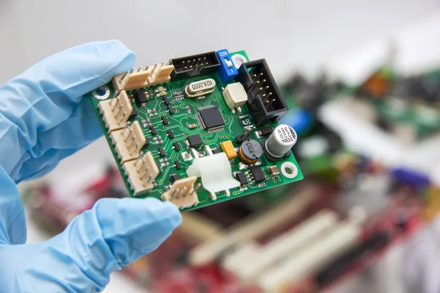
At its core, PCB power refers to the system responsible for delivering electrical energy to all components on a printed circuit board (PCB). This system, often unseen but vital, ensures that every chip, sensor, and circuit receives the appropriate voltage and current necessary for its proper operation. Effective PCB power design is paramount because it directly impacts the overall performance, reliability, and longevity of the electronic device.
A well-designed power system on a PCB minimizes losses and noise, which are critical factors to consider. Losses in power delivery cause inefficiency and heat generation. Noise on the power rails can interfere with signal integrity resulting in unreliable performance or failure of the device. A robust power system ensures that the power delivered remains consistent under various operating conditions and mitigates the risk of damage to sensitive components.
Key Considerations for PCB Power Supply Design
Effective PCB power supply design is paramount for ensuring the reliable and stable operation of electronic devices. This process involves meticulous planning and attention to several critical parameters that directly affect the quality of power delivered to all circuit components. This section delves into the core elements of PCB power supply design, emphasizing their individual importance and how they work in concert to achieve optimal circuit performance.
| Consideration | Description | Importance |
|---|---|---|
| Voltage Regulation | Maintaining a stable and consistent output voltage despite variations in input voltage or load changes. | Ensures components receive power within their specified operating range, preventing damage and malfunctions. |
| Current Carrying Capacity | The maximum amount of electrical current that a trace or power plane can safely handle without overheating or causing damage. | Prevents traces from acting as fuses and failing. Adequate current capacity is crucial for stable and reliable circuit operation. |
| Impedance Control | Managing the impedance of power supply lines to minimize signal reflections and ensure efficient power transfer. | Reduces signal reflections and noise, optimizing power delivery and enhancing the stability of the board. |
| Thermal Management | Dissipating heat generated by power components to prevent overheating, which can lead to performance degradation or failure. | Crucial for maintaining the long-term reliability of the board, preventing thermal runaways, and maintaining device performance and lifespan. |
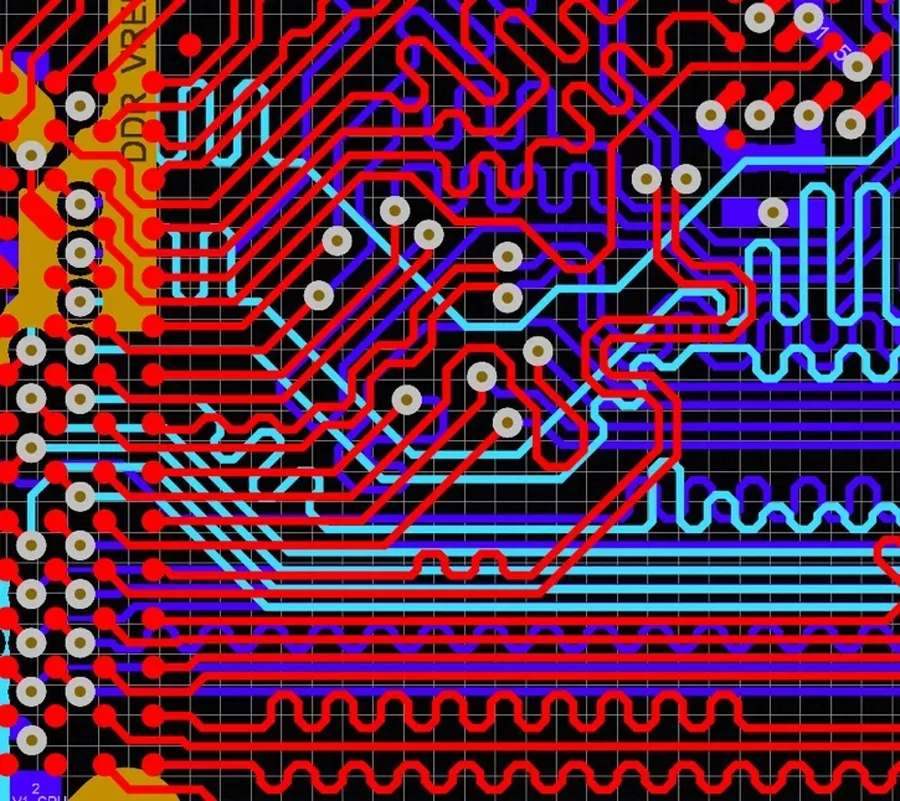
PCB Power Distribution Network (PDN) Design Strategies
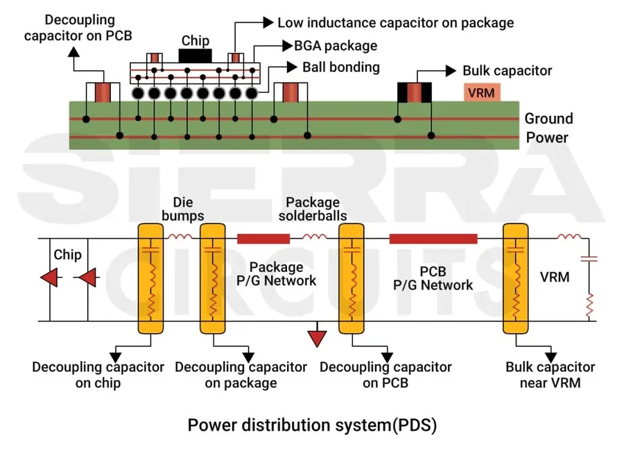
Effective design of a PCB Power Distribution Network (PDN) is crucial for ensuring stable and reliable power delivery to all components on the board. A well-designed PDN minimizes voltage drops, reduces noise, and prevents signal integrity issues, thereby maximizing the overall performance and lifespan of the electronic device.
Key strategies for PDN design include the strategic use of power planes, decoupling capacitors, and optimized trace routing techniques. Each of these elements contributes to a robust power delivery system that is capable of handling diverse load requirements and minimizing unwanted electrical disturbances.
| PDN Design Element | Purpose | Implementation Notes | Benefits |
|---|---|---|---|
| Power Planes | Provide low-impedance paths for power and ground distribution. | Use large copper areas on internal layers, typically dedicated to power and ground. | Low impedance, reduced voltage drop, excellent shielding effect. |
| Decoupling Capacitors | Reduce power supply noise and transient voltage fluctuations. | Placed close to IC power pins and at strategic points on the board. | Stable power delivery, minimized noise, improved signal integrity. |
| Trace Routing Techniques | Optimize the paths for power and ground connections. | Use wide traces, minimize trace length and impedance mismatches, and avoid abrupt changes in direction. | Reduced voltage drop, minimized impedance, lower signal reflections. |
Implementing these strategies requires a careful understanding of the specific requirements of each application. Proper planning of component placement and layer assignment can significantly improve the PDN's effectiveness.
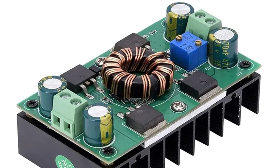
Manufacturing Techniques for High-Quality PCB Power Boards
The manufacturing of high-quality PCB power boards is a multifaceted process that demands meticulous attention to material selection, fabrication techniques, and rigorous quality control. The performance and reliability of these boards, which are critical for power delivery, are directly influenced by the manufacturing process.
| Manufacturing Step | Description | Impact on Power Delivery |
|---|---|---|
| Material Selection | Choosing appropriate substrate materials (e.g., FR-4, Rogers) and copper thickness based on the application's thermal and electrical requirements. | Directly affects current carrying capacity and thermal dissipation. Thicker copper traces reduce resistance and voltage drop. |
| PCB Fabrication | Includes steps like etching, drilling, and plating. Etching defines the copper traces, drilling creates via holes for layer connections, and plating adds conductive material to vias and pads. | Precise etching is crucial for accurate trace width and impedance control. Well-plated vias ensure reliable layer connectivity for power transfer. |
| Solder Mask Application | Application of a solder mask layer to prevent solder bridging between conductors during component soldering. | A properly applied solder mask reduces the risk of short circuits, essential for reliable power delivery systems. |
| Surface Finish | Applying a conductive finish (e.g., HASL, ENIG, Immersion silver) to the PCB pads for better solderability and corrosion resistance. | Enhances solder joint integrity, which is vital for power transmission and long-term reliability. |
| Quality Control | Involves electrical testing (continuity and isolation), visual inspection (trace alignment, plating quality), and dimensional checks to ensure compliance with design specifications. | Ensures each board meets the necessary electrical standards before deployment. This includes checks for short circuits, opens, and proper power handling. |
PCB Power and Signal Integrity: Maintaining a Clean Signal Path
Maintaining signal integrity in PCBs with power circuits is crucial for ensuring reliable performance. Power-related noise can significantly degrade signal quality, making it imperative to employ effective strategies to mitigate these effects. This section details the interplay between power and signal integrity and outlines proven techniques for maintaining a clean signal path.
The inherent challenges in mixed-signal PCB design arise from the fact that power delivery networks (PDNs) often share physical space with sensitive signal traces. Fluctuations in the power supply, known as power noise, can couple into these signal paths, leading to signal distortion, increased error rates, and potentially unreliable circuit operation. Mitigation strategies are essential to ensure consistent signal performance alongside power delivery.
| Challenge | Description | Mitigation Strategies |
|---|---|---|
| Power Noise Coupling | Fluctuations in power supply voltage can induce noise on signal lines. | Proper grounding, decoupling capacitors, and power plane design. |
| Ground Bounce | Rapid switching of high-current circuits can cause variations in ground potential. | Low-impedance ground planes, star grounding, and sufficient decoupling. |
| Electromagnetic Interference (EMI) | Power circuits can generate EMI, which can affect signal integrity. | Shielding, proper trace routing, and filtering techniques. |
| Impedance Mismatch | Inconsistent impedance across power and signal paths can lead to reflections and signal degradation. | Controlled impedance routing, proper termination, and impedance matching components. |
Several strategies are effective for mitigating the impact of power noise on signal integrity. These primarily revolve around managing impedance, controlling noise, and preventing unwanted coupling.
- Proper Grounding Techniques
Establishing low-impedance ground paths is critical. This often involves utilizing a dedicated ground plane, star grounding configurations, and minimizing ground loops. A well-defined ground plane provides a stable reference potential and reduces common-mode noise. - Strategic Decoupling Capacitors
Decoupling capacitors placed close to power pins of integrated circuits act as local energy storage, reducing voltage fluctuations caused by current demand changes. These capacitors must be chosen to operate effectively over a range of frequencies. - Shielding
Implementing shielding techniques can minimize EMI coupling between power and signal traces. Shielding may involve using grounded layers or enclosures, as well as careful trace routing to minimize parasitic capacitance and inductance. - Isolation Techniques
Galvanic isolation between the power and signal circuits can block common-mode noise. Isolation transformers or opto-isolators are used where direct electrical connections are not desired or are hazardous. - Controlled Impedance Routing
Matching the impedance of signal traces to the source and load impedance minimizes signal reflections and ensures that the signal is transmitted correctly, preventing signal degradation and loss. - Filtering
Using filtering components, such as ferrite beads and common-mode chokes, can suppress high-frequency noise on power lines before it can couple into signal paths.
PCB Power Applications Across Industries
The versatility of PCB power solutions is evident in their widespread adoption across diverse industries. From powering handheld devices to supporting critical infrastructure, PCBs are integral to the functionality of countless electronic systems. This section will explore several key application areas, highlighting the specific requirements and impact of PCB power in each sector.
Below, we explore how PCB power is implemented and what specific needs are met in various industries:
- Consumer Electronics
PCBs are the backbone of most consumer electronic devices, such as smartphones, tablets, laptops, and gaming consoles. These applications require compact, efficient power delivery with minimal noise to maintain optimal performance and battery life. Power management ICs and multilayer PCBs are frequently utilized to achieve these goals. - Medical Equipment
In the medical field, PCB power is critical for devices like diagnostic imaging equipment (MRI, X-ray), patient monitoring systems, and implantable devices. These systems demand highly reliable and stable power supply with stringent safety standards and minimal electromagnetic interference (EMI). Often, specialized materials and manufacturing processes are employed to meet medical-grade requirements. - Automotive Industry
Automotive applications leverage PCBs for engine control units (ECUs), infotainment systems, advanced driver-assistance systems (ADAS), and electric vehicle (EV) power management. These demanding environments require PCBs that can withstand harsh conditions like extreme temperatures, vibration, and shock. High-current handling and robust thermal management are key design considerations. - Aerospace
Aerospace applications, including satellites, aircraft avionics, and guidance systems, require exceptionally reliable PCB power systems. These systems need to function under extreme conditions like vacuum, high radiation, and wide temperature variations. Lightweight materials and redundant power architectures are common in these applications. Stringent quality assurance processes are crucial to ensure mission success. - Industrial Automation
PCB power is essential in industrial settings for powering programmable logic controllers (PLCs), motor drives, sensors, and other automation equipment. Robust and reliable power delivery is essential in this sector. PCBs used in industrial automation must often withstand challenging environmental factors such as dust, moisture, and high temperatures, and must provide excellent electrical isolation and noise reduction capabilities. - Telecommunications
Telecommunications infrastructure, including base stations, routers, and switches, relies on robust PCB power for uninterrupted operation. High-density PCBs with advanced thermal management capabilities are used for efficient power delivery and heat dissipation. Redundancy and fail-safe designs are critical in telecommunication systems. - Renewable Energy Systems
In renewable energy, PCBs are essential for solar inverters, wind turbine controllers, and battery management systems. High-efficiency power conversion and robust operation in outdoor conditions are crucial. These applications often use high-power PCBs with effective thermal management to handle the high currents generated by renewable energy resources.
Frequently Asked Questions About PCB Power
This section addresses common questions regarding PCB power, providing clear and concise answers to help you better understand this critical aspect of electronics design and manufacturing. We'll cover fundamental concepts, terminology, and common industry practices.
- What exactly is a power PCB?
A power PCB, or power printed circuit board, is a specialized type of PCB designed to handle and distribute electrical power efficiently and reliably to various components. Unlike signal PCBs that primarily manage data transmission, power PCBs are optimized for current carrying capacity, voltage regulation, and thermal management to ensure that all parts of the circuit receive the necessary power for proper operation. This often includes features such as thicker copper traces, dedicated power planes, and careful thermal design to handle the heat generated by power distribution. - What does PCB stand for?
PCB stands for Printed Circuit Board. It is a non-conductive substrate, typically made of fiberglass or composite materials, onto which conductive pathways are etched or printed. These pathways, usually made of copper, connect various electronic components, allowing electrical signals and power to flow between them. PCBs provide a physical structure for mounting components and a defined electrical pathway, making the creation of complex circuits easier and more efficient. - What is the primary electrical function of a PCB?
The primary electrical function of a PCB is to provide a structured platform for mounting electronic components and facilitate electrical connections between them. It acts as the foundational structure for the assembly of an electronic circuit. Beyond just physical support, the copper traces on a PCB serve as conductive paths for both electrical signals and power, enabling devices to function as designed. The careful design of the PCB layout is critical for ensuring proper circuit performance and minimizing signal interference. - How does power distribution differ on a signal PCB versus a power PCB?
While both signal and power PCBs utilize conductive traces, their approach to power distribution differs substantially. Signal PCBs are typically optimized for the transmission of low-current signals and focus on maintaining signal integrity. Power PCBs, in contrast, are designed for delivering higher current levels and often feature thicker copper traces, dedicated power planes, and larger vias to handle the current and minimize voltage drops. Power PCBs also have critical thermal considerations to manage the heat generated during power distribution. - What are common voltage regulation methods used on power PCBs?
Voltage regulation on power PCBs is essential for ensuring that components receive a stable and consistent voltage supply. Common methods include linear regulators, switching regulators (such as buck, boost, and buck-boost converters), and low-dropout (LDO) regulators. Switching regulators are favored for their efficiency in handling larger voltage differences and providing higher power delivery, while LDO regulators are used when a small difference exists between input and output voltages and when low noise is critical. - Who are some of the leading manufacturers in the PCB power industry?
The PCB power industry is supported by a range of manufacturers known for their quality and innovation. Some leading names include companies like TTM Technologies, known for its advanced PCB manufacturing capabilities; Jabil, a multinational provider of electronics manufacturing services; and Flex, another global manufacturing services provider; other manufacturers include companies like, Kingboard Chemical Holdings, and Multek, are also recognized for their power-focused PCBs. In addition, local specialized PCB manufacturers may also provide excellent power PCB solutions based on specific region and project needs. - Why is thermal management critical for PCB power?
Thermal management is crucial for PCB power because the flow of current generates heat, which can negatively affect performance and reliability of electronic components, and in extreme cases, cause damage or failure. Effective thermal design includes the use of heat sinks, thermal vias, and proper layer stack-up to dissipate heat efficiently, thereby ensuring the longevity and stable operation of the PCB and the electronic devices it powers. Overheating can cause components to malfunction, leading to system failures, reduced life spans, and even safety issues.
Troubleshooting and Debugging Common PCB Power Issues
Effective troubleshooting of PCB power issues is crucial for maintaining the reliability and performance of electronic devices. Addressing problems such as voltage drops, current overloads, and short circuits requires a systematic approach that combines careful diagnostics and preventive maintenance. Understanding the root causes of these issues allows for targeted interventions to restore optimal functionality.
- Voltage Drops
Voltage drops occur when there is a loss of voltage along a conductive path. This can be caused by excessive resistance in traces, poor connections, or insufficient power supply capacity. To troubleshoot, measure voltage at various points in the circuit to identify where the drop is occurring, and then inspect the related components and traces. Consider using wider traces or increasing power supply capabilities to mitigate the issue. - Current Overloads
Current overloads happen when the current flowing through a component or trace exceeds its rated capacity, leading to overheating and potential damage. Check datasheets to ensure components are operated within their specified limits. Measure current in the circuit, and identify the source of high consumption. Reduce current draw by optimizing the design or adding protective devices like fuses. - Short Circuits
Short circuits are unintended low-resistance paths that cause excessive current flow, often resulting in immediate failures. Visually inspect the board for solder bridges or damaged insulation. Use a multimeter to check for continuity between unintended points in the circuit. Repair short circuits by isolating the affected area and correcting the faulty connection; thorough testing is crucial following a repair. - Component Failures
Component failures can manifest as unexpected behaviors, such as overheating, intermittent operation, or complete malfunction. Begin by visually inspecting components for any physical damage. Verify the integrity of the components' functionality using appropriate test equipment. Replace any defective components with ones that meet the original design specifications. - Thermal Issues
Excessive heat buildup can cause components to malfunction or degrade over time. Examine the thermal design of the board, focusing on heatsinks, airflow, and component placement. Monitor component temperature using thermal imaging or thermocouples. Add or enhance heatsinks, optimize airflow, or relocate components with significant thermal output.
The Future of PCB Power: Trends and Innovations
The evolution of PCB power technology is driven by the relentless pursuit of enhanced efficiency, miniaturization, and performance. Innovations in materials, design methodologies, and manufacturing techniques are converging to create more powerful, compact, and reliable electronic devices. The future of PCB power is focused on meeting the ever-increasing demands of next-generation electronics, from portable devices to high-performance computing systems.
- Advanced Materials
The industry is exploring new substrate materials with improved thermal conductivity and reduced dielectric losses. Materials like advanced ceramics, composites, and polymers with tailored electrical properties are being investigated to enhance power handling capabilities and minimize energy waste. - Integrated Power Management
The trend is towards integrating power management functions directly onto the PCB. This approach, utilizing advanced IC packaging and embedded passives, minimizes the footprint of power circuitry, reduces parasitic inductance, and facilitates more efficient power delivery. Power modules are also being developed to enhance efficiency and reduce PCB area. - Advanced Cooling Techniques
As power density increases, efficient thermal management is paramount. Innovations such as embedded heat spreaders, microfluidic cooling channels, and advanced thermal interface materials are being developed to effectively dissipate heat and maintain optimal operating temperatures, preventing performance degradation and ensuring system reliability. - Digital Power Control
Digital control loops offer more flexibility, precise voltage regulation, and power saving advantages. This trend allows for dynamic adjustment of power parameters depending on the operating state and overall improvements in system performance. Digital control also facilitates easier integration into smart power management systems. - High-Density Interconnect (HDI) Technologies
HDI technology is becoming crucial for integrating more power components into smaller footprints. Features such as microvias and fine lines enable denser circuitry, thereby reducing board size while improving electrical performance. This allows for smaller, more efficient power circuits. - Wireless Power Transfer
Emerging applications are now integrating wireless power transfer capabilities directly onto the PCB. This eliminates the need for physical connectors for certain applications allowing for more versatile and compact designs. The continued improvement in inductive coupling efficiency and power transfer rates will drive adoption.
In conclusion, understanding 'PCB power' is fundamental to mastering the design and functionality of electronic devices. From meticulous planning during the design phase to precise manufacturing, every step is crucial in ensuring a stable and efficient power supply for PCB components. As technology evolves, so will the demands on PCB power systems, making continued innovation and research in this field vital. Ultimately, the power of the PCB lies in its ability to efficiently manage electrical energy, enabling the diverse range of applications we rely on daily, shaping the future of electronics and beyond.