Your Complete Guide to a Successful PCB Order
In today's rapidly evolving electronics landscape, printed circuit boards (PCBs) are the backbone of virtually every device we use. Understanding how to navigate the PCB order process is crucial for makers, engineers, and businesses alike. This guide will walk you through each step, from initial design considerations to selecting the right manufacturing partner for your PCB order, ensuring a successful project outcome.
Understanding Your PCB Order Needs
Before initiating a PCB (Printed Circuit Board) order, a thorough understanding of your project's specific requirements is paramount. This initial step dictates the entire manufacturing process and ensures the final product meets the intended application's demands. Defining these needs precisely prevents costly errors, delays, and the potential for non-functional boards.
At the heart of this task lies the necessity of detailed planning and accurate specification, which is critical for a successful PCB order. The user's intent is to ensure that the final PCB meets the design requirements and functions correctly in the intended application. Key information needed includes functionality of the PCB, physical dimensions, layer count, material specifications, any specific features, and environmental conditions. Possible solutions would be to go through the specifications with a detailed checklist, consulting with electrical engineers to go through the design constraints, researching existing applications and using design tools to model the required behaviour. The advantage of a well-defined PCB order is a decrease in production errors, faster production times and better functioning boards, the disadvantages are the time needed in initial planning and the need for deep expertise in electronics.
- Functionality
Clearly articulate the PCB's purpose. What functions will it perform? What type of electronic circuits it will be supporting? What is the role of the PCB in the overall system, and what critical components are included? - Physical Dimensions
Specify the exact dimensions (length, width, and thickness) required for the PCB. Factor in any constraints of the enclosure or system it will be integrated into. Consider tolerances for fitment. Any height restrictions on the component side should also be mentioned. - Layer Count
Determine the number of conductive layers needed. Single-layer PCBs are suitable for simple designs, while multilayer PCBs are necessary for complex circuits. More layers generally provide higher routing flexibility and better signal integrity, but also increases the cost. - Material Specifications
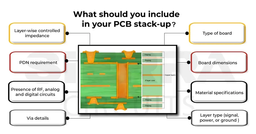
Select the appropriate substrate material (e.g., FR-4, aluminum, polyimide). FR-4 is a popular material known for its balance of cost and performance, and consider the dielectric constant and thermal characteristics. - Special Features
Identify any special requirements like impedance control for high-speed signals or controlled impedance transmission lines. Also the type and size of the vias, plating finishes (e.g., HASL, ENIG), solder mask colours, silkscreen requirements, and any other non-standard specifications. Note also any specific requirements for thermal management that must be incorporated into the design. - Environmental Conditions
Specify the operating environment of the PCB. Is it intended for harsh conditions with extreme temperatures, humidity, or mechanical stress? This will influence material choices and reliability considerations.
| Consideration | Description | Impact on PCB Order |
|---|---|---|
| Functionality | The intended task of the PCB. | Determines PCB layer requirements and type of components. |
| Physical Dimensions | The size of the board. | Affects material quantity and manufacturability. |
| Layer Count | Number of conductive layers. | Impacts complexity and cost. |
| Material | Type of PCB substrate. | Influences cost and performance. Also affects the operating temperatures. |
| Special Features | Specific requirements like impedance control. | Demands specific manufacturing processes. Affects costs and time. |
| Environmental Conditions | Temperature, humidity and mechanical stress in operating conditions. | Influences material choice and overall reliability. May require extra testing and inspection. |
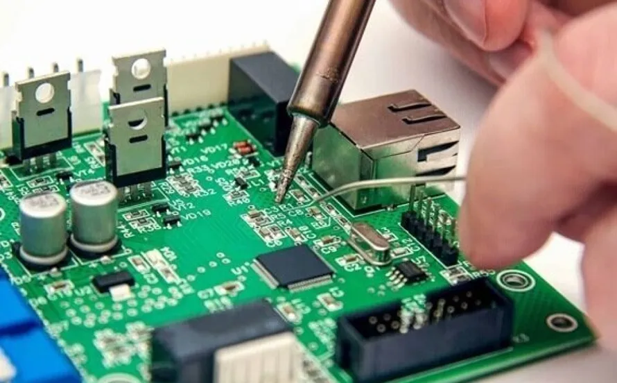
Preparing Your PCB Design Files
The precision and accuracy of your PCB design files are paramount to the success of your PCB order; these files, primarily Gerber files, are what manufacturers use to produce your boards. Incorrect or incomplete files can result in significant delays, increased costs, or unusable PCBs, so adherence to industry standards and thorough file verification is essential.
Key aspects of PCB design file preparation include:
- File Format Standards
Gerber files (RS-274X format) are the industry standard for PCB manufacturing. Other file types such as Excellon drill files and IPC-D-356 netlists are also necessary to convey complete PCB specifications. Always check with your manufacturer for any specific file format preferences. - Design for Manufacturability (DFM)
DFM analysis involves the comprehensive assessment of your PCB design to identify any features that might cause manufacturing problems. This includes things like minimum trace widths and spacing, hole sizes, and pad clearances. These checks are crucial for ensuring your design can be reliably and efficiently fabricated. - Layer Mapping
Each layer in your PCB (copper layers, solder mask, silkscreen) must be accurately represented in its respective Gerber file. Proper layer mapping prevents incorrect board fabrication. It is crucial that you generate all necessary files, including but not limited to: Top and Bottom copper layers, Solder Mask, Silk Screen, Board outline, Drill files, etc. - Aperture and Tooling Tables
Aperture tables are necessary for older Gerber formats; if you're using RS-274X, aperture information is included within the Gerber files, simplifying the process. However, using the correct tooling definitions for drills is crucial as well. Confirm the required drill sizes with your manufacturer. - Avoiding Common Errors
Pay close attention to design elements like trace widths, clearances, vias and soldermask clearances. Incorrect or mismatched units (e.g., mm vs. inches), lack of a clearly defined board outline and the absence of important layers like solder mask or silkscreen, can lead to costly rework.
| File Type | Description | Importance |
|---|---|---|
| Gerber (RS-274X) | Image files of each PCB layer. | Critical for defining copper, soldermask, and silkscreen patterns. |
| Excellon Drill Files | Contains coordinates and sizes for all drill holes. | Essential for creating through-holes, vias, and mounting holes. |
| IPC-D-356 Netlist | Text file describing the electrical connectivity of the circuit. | Necessary for netlist testing, crucial for complex boards. |
| Readme/Instruction file | A simple text file detailing any board specifications, layer order, material specifications, stackup, special instructions, or other notes. | Very helpful for the PCB manufacturer to understand the specifics of your board. |
By paying close attention to each of these elements and conducting thorough DFM checks, you can substantially reduce the risk of errors and delays in your PCB order, ultimately leading to a higher quality end product.
Choosing the Right PCB Manufacturer
Selecting the appropriate PCB manufacturer is a pivotal decision that can significantly impact the success of your electronics project. This choice involves carefully evaluating several critical factors to ensure that the manufacturer can meet your specific requirements regarding cost, quality, and production timelines.
A proper assessment of the manufacturer's capabilities, pricing, lead times and customer service is necessary to avoid potential project delays and budget overruns. This chapter provides a comprehensive approach to help you confidently choose the ideal partner for your PCB fabrication needs.
- Pricing Structure
Compare quotes from different manufacturers, considering not just the base price but also any additional charges for tooling, setup, testing, and shipping. - Production Capabilities
Verify the manufacturer's ability to produce PCBs that meet your project’s specifications, including layer count, board thickness, material type (e.g., FR-4, aluminum, flexible), minimum trace width/spacing, and special treatments like impedance control or gold plating. - Lead Times
Assess the typical production lead time to ensure that it aligns with your project's timelines. Consider also the expedited services, if available, and their additional cost. - Specialization
Some manufacturers specialize in specific types of PCBs (e.g., high-frequency, flexible, or high-density interconnect boards). Ensure the manufacturer's expertise matches your project's specific requirements. - Customer Support
A manufacturer that provides prompt, clear communication is essential. Evaluate the availability and responsiveness of customer support in addressing your questions, issues, or concerns. - Reviews and Reputation
Research customer reviews, testimonials and reputation. Look for consistent feedback regarding the quality of the PCBs produced and the manufacturer’s reliability.
| Factor | Description | Importance |
|---|---|---|
| Pricing | Total cost including setup, tooling, and shipping. | High - Budgetary constraints are crucial. |
| Production Capabilities | Ability to meet required specifications. | High - Project functionality depends on it. |
| Lead Times | Time from order to delivery. | Medium - Affects project timelines. |
| Specialization | Expertise in particular PCB types. | Medium - For specialized project needs. |
| Customer Support | Responsiveness and clarity of communication. | Medium - Facilitates smooth production. |
| Reviews & Reputation | Past customer experiences & reliability. | High - Predicts service quality. |
For projects involving complex and advanced PCBs, selecting a manufacturer with demonstrated experience and state-of-the-art facilities is critical. In contrast, for more standard PCB applications, smaller shops may be sufficient, often at lower cost. Understanding the specific requirements of your project will guide this crucial choice to avoid potential problems.
Cost Factors for PCB Orders
Understanding the various cost drivers in PCB manufacturing is essential for effective budget planning and project management. The final price of a PCB order is influenced by a multitude of factors, each of which needs careful consideration during the design and order placement stages. These factors range from fundamental board characteristics to specialized manufacturing processes.
| Cost Factor | Description | Impact on Cost |
|---|---|---|
| Board Size | The physical dimensions of the PCB. | Larger boards require more material and processing time, increasing cost. |
| Material Type | The base material used for the PCB (e.g., FR-4, Aluminum, Rogers). | Advanced materials with better performance (e.g., high-frequency laminates) are more expensive. |
| Layer Count | The number of conductive layers in the PCB. | More layers increase complexity and processing time, significantly raising the cost. |
| Quantity | The number of PCBs in the order. | Larger orders generally benefit from economies of scale, resulting in a lower per-unit cost. |
| Lead Time | The time required to manufacture the PCBs. | Shorter lead times, often called express services, typically incur higher costs. |
| Special Processes | Additional manufacturing processes such as via tenting, gold plating, impedance control or blind/buried vias. | These processes add complexity and cost, depending on the type. |
| Panelization | The arrangement of multiple PCBs on a single production panel. | Panelization can reduce per-unit cost by optimizing board layout, but requires additional engineering effort. |
It's crucial to evaluate the trade-offs between cost, performance, and delivery timelines during the design phase. Engaging with your manufacturer early in the design process for a Design for Manufacturability (DFM) review can also mitigate potential cost overruns due to unforeseen manufacturing challenges. Below, we explore each of these factors in detail:
- Board Size and Complexity:
Larger boards use more materials and take more processing time, increasing costs. Likewise, complex layouts with high component densities often increase cost due to manufacturing challenges. - Material Selection
The material (e.g., FR-4, Aluminum, Rogers) directly affects performance and cost. High-performance materials are more expensive but offer advantages like better thermal or electrical characteristics. - Layer Count:
The number of layers significantly impacts the cost. More layers increase complexity, require precision alignment during manufacturing, and therefore increase prices. - Order Quantity:
The quantity ordered greatly influences the unit price due to the set-up costs in production, high-quantity orders often significantly reduce the per-unit price. - Lead Time:
Shorter manufacturing lead times are usually associated with increased prices. Standard production lead times are less expensive but take longer, which should be factored into project timelines. - Special Manufacturing Processes:
Special processes like controlled impedance, gold plating, or specific via types require specialized equipment and processes which can significantly increase the price.
Navigating the PCB Order Process
Successfully navigating the PCB order process is crucial to ensure your project’s timely and cost-effective completion. This involves a series of well-defined steps, beginning with the preparation of your design files and culminating in the delivery of your manufactured PCBs.
- File Upload and Design Review:
Upload your Gerber files (and any necessary drill files, netlists) to the manufacturer's website. Most manufacturers offer online tools to review your design, automatically detecting potential errors or manufacturability issues such as minimum trace widths, via sizes, or clearances. Pay close attention to any warnings and address them before proceeding. - Specification Selection:
Choose the required PCB specifications including material type (FR4, aluminum, etc.), layer count, board thickness, copper weight, surface finish (HASL, ENIG, etc.), solder mask color, and silkscreen color. Ensure all specifications match your design requirements. Refer to your design specifications and select the appropriate materials for your application. Consider performance characteristics such as dielectric constant and thermal properties. - Instant Quote and Price Review:
Most PCB manufacturers offer an instant quote based on the uploaded files and selected specifications. Review the costs for various options, including different quantities, and lead times, and select what best suits your budget and timeline. Factor in potential additional costs for expedited services or more complex manufacturing requirements. - Order Confirmation:
Carefully review the order summary before finalizing and submitting the order. Confirm all specifications and quantities, ensure that your shipping address is correct, and that you understand the payment terms. Note the expected shipping date. Double-check that the specifications match your design files and that you are getting exactly what you require. - Production Tracking
Once your order is placed, manufacturers usually offer a tracking system to monitor the different stages of PCB fabrication, from CAM processing, fabrication, and assembly, to packaging. Stay updated on progress, especially if lead times are tight. Most manufacturers will provide regular updates as the boards move through each stage. - Post-Production Monitoring:
After the production of PCBs, many manufacturers will ship the order. Be aware of the expected shipping date and ensure arrangements are in place for receiving the PCBs. Check the delivery for physical damage. In the event of a delay, contact the manufacturer promptly to determine the reason and to discuss solutions.
Throughout this process, maintain clear communication with the PCB manufacturer, ask clarifying questions, and address any concerns immediately. Thoroughness and attention to detail are key to a successful PCB order.
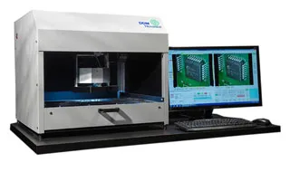
Quality Control and Inspection of Your PCBs
Ensuring the quality of your printed circuit boards (PCBs) is critical for the functionality and reliability of your electronic devices. This section details the essential inspection criteria and procedures, both those employed by manufacturers and those you should perform upon receiving your boards, to identify defects and confirm adherence to specifications.
Rigorous quality control is not just about finding flaws; it’s about preventing future issues, saving time and resources in the long run. Understanding these checks will empower you to ensure you receive PCBs that meet your project's precise requirements.
| Inspection Area | Manufacturer Checks | User Checks |
|---|---|---|
| Dimensional Accuracy | Automated optical inspection (AOI) for precise measurements against design files. | Verify overall dimensions using calipers and compare to design specifications. |
| Layer Alignment | X-ray and cross-section analysis to verify precise layer registration. | Visually check for misalignments of layers around edges and through holes, using magnifying glass if necessary. |
| Solder Mask and Silkscreen | AOI checks for proper coverage and alignment of solder mask and silkscreen. | Check that solder mask fully covers intended areas and prevents solder bridges, confirm legibility of silkscreen component markings. |
| Etch Quality | Microscopic inspection and cross-sections to assess the integrity of etched traces. | Look for consistent trace width and proper copper removal from non-trace areas. |
| Plating and Finish | Chemical analysis and thickness measurements to ensure correct plating and finish. | Check that plating is consistent and there are no visible oxidation or contamination. Ensure gold plating is applied correctly if specified. |
| Drilled Holes | Automated inspection for hole size and position accuracy. | Confirm that all holes are present, correctly sized and positioned, check that via holes are plated through properly. |
| Electrical Test | Flying probe or bed-of-nails testing to check for shorts and open circuits. | Perform continuity and impedance testing if appropriate, checking for shorts and opens. |
Understanding the above table will help both you and the manufacturer achieve a higher level of quality for your PCB.
- Common PCB Defects to Identify
Be vigilant for common defects including: solder mask misalignments, broken traces, insufficient plating, missing vias, and shorts between traces. These issues can often be identified through visual or basic electrical testing. - What to do when a defect is identified
If defects are found, document them thoroughly with photographs and descriptions. Contact the PCB manufacturer immediately to discuss the issue and explore possible solutions, such as replacement or rework, adhering to any warranty or return policies.
Frequently Asked Questions About PCB Orders
This section addresses common questions and concerns that arise during the PCB ordering process, providing clear and concise answers to guide you through potential challenges and uncertainties.
- What is the typical lead time for PCB production?
Lead times for PCB production can vary significantly depending on several factors, including the complexity of the design, the quantity ordered, the manufacturer's current workload, and the selected shipping method. Standard lead times often range from a few days to several weeks. Manufacturers typically offer expedited options for quicker turnaround, albeit at a higher cost. Always confirm lead times with your chosen manufacturer before finalizing your PCB order. - How can I ensure the confidentiality of my PCB designs?
Protecting your intellectual property is crucial. Start by selecting a PCB manufacturer with a strong reputation for confidentiality. Reputable manufacturers will have strict non-disclosure agreements (NDAs) in place that explicitly define their obligations regarding your design files and any information related to your project. Also, consider watermarking your designs and utilizing secure file transfer protocols. - What are some common PCB fabrication errors to avoid?
Common PCB fabrication errors include inadequate copper clearance, incorrect drill sizes for vias, insufficient solder mask registration, and missing or incorrectly specified silkscreen details. To avoid these, rigorously perform design rule checks (DRCs) before submitting files, review all fabrication files with a careful attention to detail, and clarify any uncertainties with your manufacturer. - How should I handle issues that arise during PCB fabrication?
If issues arise during PCB fabrication, the first step is to communicate promptly and clearly with the manufacturer. Provide detailed information about the issue, including specific errors noted, and supporting images if available. Most reputable manufacturers are willing to work with you to address problems, this may involve design revisions, or remanufacturing. Keep records of all communication. If the manufacturer is not responsive or unable to rectify the issues, you can escalate the concern, or seek a refund. - What should I do if the ordered PCBs do not meet specifications?
If delivered PCBs do not meet your specifications, immediately inform the manufacturer and provide clear, detailed documentation of the discrepancies. Compare the received boards with your design files and relevant fabrication specifications. Depending on the severity of the errors, you may be able to have the manufacturer correct the errors by re-manufacture the boards. If the manufacturer is unwilling to resolve the issue, you may need to explore other avenues such as a chargeback, or consider seeking resolution through legal means. - What file formats are required for PCB orders?
The standard file formats for PCB orders are Gerber files (RS-274X or X2 format), which provide a graphical representation of each layer of your PCB, along with NC Drill files for drilling information. For some manufacturers, centroid data and a bill of materials may be required for assembly services. Ensure all of your files are compatible with the manufacturer's requirements. - How to select the right PCB material for your design?
Selecting the right material is crucial for a PCB design. Different materials such as FR-4, CEM-1, Rogers, etc., have different electrical and mechanical properties, such as dielectric constant, thermal conductivity, flexural strength. The choice of material also affects the cost, temperature performance, and signal integrity. Choose a material that meets the specific requirements of your application.
Future of PCB Ordering: Trends and Innovations
The printed circuit board (PCB) manufacturing landscape is constantly evolving, driven by technological advancements and increasing demands for higher performance and sustainability. This section explores key trends and innovations poised to reshape the future of PCB ordering, enabling engineers to stay ahead of the curve and optimize their designs for emerging applications.
Here's a look at some of the most significant trends:
- Advanced Materials
The development and adoption of new substrate materials, such as ceramics, composites, and advanced polymers, are enabling PCBs to operate at higher frequencies, withstand extreme temperatures, and offer improved electrical and mechanical properties. These materials are critical for applications in aerospace, automotive, and high-speed computing. - Enhanced Precision and Miniaturization
Driven by the demand for smaller and more powerful devices, PCB manufacturing techniques are pushing the boundaries of precision. This includes the development of finer line widths and spaces, microvias, and other technologies that enable higher component density and improved signal integrity. Innovations in laser direct imaging (LDI) and advanced etching processes are key to achieving these levels of miniaturization. - Sustainable Production Practices
Environmental concerns are driving a shift towards more sustainable PCB manufacturing practices. This includes the use of eco-friendly materials, reduced water consumption, and the adoption of closed-loop recycling systems. Manufacturers are also exploring alternative plating techniques that reduce the use of hazardous chemicals. These practices align with global environmental initiatives and customer demand for greener products. - Additive Manufacturing (3D Printing) for PCBs
Additive manufacturing, or 3D printing, is emerging as a promising technology for PCB prototyping and low-volume production. 3D-printed PCBs offer greater design flexibility, rapid prototyping capabilities, and the potential for customized and complex geometries. While still in development, this technology has the potential to disrupt traditional PCB manufacturing workflows, especially for niche applications. This technology has the potential to lower the barrier to entry for electronics prototyping and enable rapid design iterations. - Smart Manufacturing and Automation
The incorporation of smart manufacturing concepts like machine learning, AI, and automation in PCB fabrication processes will lead to enhanced production yields, decreased human mistakes, and higher efficiency. These advancements in process control and automation will help in making PCBs faster, with increased reliability and reduced costs. - Embedded Components
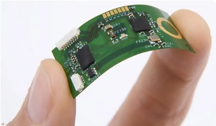
The practice of embedding passives and even active devices within the PCB layers is gaining traction. This approach optimizes space utilization, reduces board size, enhances thermal management and can improve electromagnetic compatibility. Advanced lamination technologies are required to make this integration a reality. - Flexible and Wearable Electronics
The growing market for wearable electronics has spurred the development of flexible PCBs that can conform to curved surfaces and dynamically bend. These flexible circuit boards use materials like polyimide and transparent conductive films. The development of new substrates and deposition methods will drive the expansion of this market.
These trends collectively point towards a future of PCB manufacturing that is more flexible, precise, and eco-conscious. PCB engineers can take advantage of these advancements by:
- Staying informed on materials.
Keeping up-to-date with the newest materials and evaluating their compatibility with the particular needs of their designs. - Optimizing designs for miniaturization.
Embracing miniaturization techniques will ensure their designs are compatible with advanced manufacturing capabilities and can deliver high performance. - Choosing suppliers with sustainable practices.
Partner with suppliers that follow sustainable practices in their production processes. This will help not only the environment but can also contribute to a competitive edge. - Exploring the possibilities of additive manufacturing.
As the technology develops further, look at 3D printing for prototyping and possibly for low volume production applications. - Investing in automation and smart manufacturing principles.
This will lead to better outcomes in production yields and reduce manufacturing costs.
Ordering PCBs doesn't have to be a daunting task. By carefully considering your design requirements, choosing the right manufacturer, and following the best practices outlined in this guide, you can streamline the process and ensure a high-quality outcome for your PCB order. Whether you are a hobbyist or a large corporation, understanding these steps is key to successful electronics projects. Remember to always plan and do your due diligence for every PCB order you intend to make.