The TDA2030 amplifier circuit is a cornerstone for DIY audio enthusiasts, offering a robust and cost-effective solution for building hi-fi audio amplifiers. This article delves into the intricacies of the TDA2030, guiding you through its design, implementation, and optimization, making it easy for anyone to create their own sound system. Just like a conductor leading an orchestra, understanding the TDA2030 is key to harnessing powerful audio.
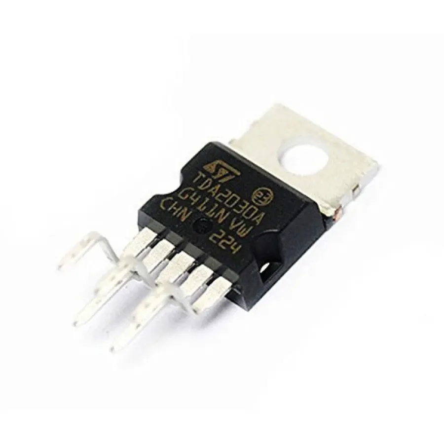
The TDA2030 is a monolithic integrated circuit intended for use as a low-frequency class AB amplifier, commonly used in audio amplification due to its robust performance and ease of implementation. Key features include its ability to deliver significant power output with relatively low distortion, making it suitable for various applications from basic amplifiers to more complex audio systems. It offers internal protection against short circuits, thermal overloads, and load dumps, enhancing its reliability and robustness.
| Feature | Specification | Details |
|---|---|---|
| Power Output | Up to 14W | Typically at 4Ω load with ±14V supply, actual output power depends on supply voltage and load impedance. |
| Operating Voltage | ±6V to ±22V (Dual Supply) | Wide range of operating voltage, allowing flexibility in power supply design. Can also operate with single supply but with reduced performance |
| Peak Output Current | Up to 3.5A | Capability of providing large currents for short durations, enabling it to drive low impedance loads. |
| Frequency Response | 20Hz to 20kHz | Capable of amplifying the full audible range, making it suitable for Hi-Fi audio amplification |
| Total Harmonic Distortion (THD) | Typically 0.5% at 10W | Low THD ensures high fidelity audio signal reproduction. |
| Input Impedance | 100kΩ | High input impedance to avoid loading the input signal source. |
| Protection | Short Circuit, Thermal Overload | Robust protection features to prevent damage from common operational faults. |
| Pin Configuration | 5-Pin Package (Pentawatt) | Standard pinout includes Non-Inverting Input, Inverting Input, Output, Vcc, and GND. |
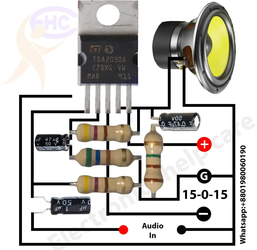
Constructing a functional TDA2030 amplifier circuit involves careful selection and arrangement of passive components alongside the integrated circuit. This section details the fundamental design principles and component choices required for a basic amplifier implementation, emphasizing a common 12V configuration.
The core of the TDA2030 amplifier design comprises the following essential components:
A typical basic TDA2030 amplifier circuit can be set up with the following considerations:
For a 12V implementation, the TDA2030 can be powered directly from a regulated 12V power supply. It is important to select components that can withstand the voltage and current requirements. For instance, a 12V implementation will have different resistor values compared to another configuration. The key point is to tailor component values for the desired gain and frequency response.
| Component | Function | Typical Value for 12V Supply |
|---|---|---|
| TDA2030 IC | Amplification | 1 (Single) |
| Input Capacitor | DC Blocking | 1-10 uF |
| Feedback Resistors (Gain) | Set gain of amplifier | 10kΩ, 1kΩ (for gain of 10) |
| Output Capacitor | DC Blocking | 220-470 uF |
| Bypass Capacitor | Power supply filtering | 100nF |
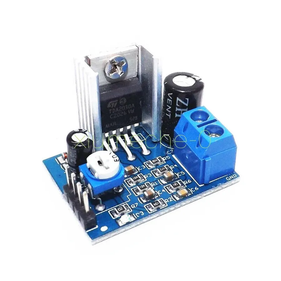
The TDA2030 amplifier IC can be powered using either a single or a dual power supply configuration. While both are viable, they present distinct characteristics that influence the amplifier's performance, particularly in terms of signal swing and dynamic range. The selection between these configurations directly impacts the amplifier’s ability to reproduce audio signals accurately and efficiently.
| Feature | Single Power Supply | Dual Power Supply |
|---|---|---|
| Signal Swing | Limited to half the supply voltage | Full supply voltage range (positive and negative) |
| Dynamic Range | Reduced due to limited signal swing | Increased providing better fidelity |
| Distortion | Higher distortion at higher power outputs due to signal clipping | Lower distortion due to symmetrical signal swing |
| Complexity | Simpler circuit design | Slightly more complex due to the addition of a negative rail |
| Output DC Offset | Requires DC blocking capacitor in series with the speaker | Can operate without a DC blocking capacitor, reducing component count |
| Applications | Cost-effective, suitable for low-power applications where some signal fidelity may be sacrificed | Higher fidelity audio applications, including high-performance audio systems and pre-amplifiers. |
In summary, choosing between a single and dual power supply configuration depends on the application's requirements. The dual supply provides superior performance, reduced distortion, and improved dynamic range, making it suitable for high-fidelity applications. Conversely, the single supply is simpler and more cost-effective but compromises on signal quality.
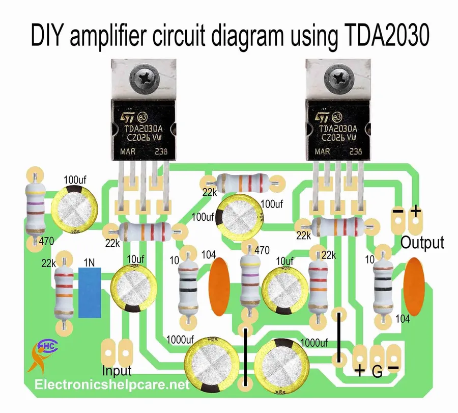
This section provides detailed circuit diagrams and schematics for various TDA2030 amplifier configurations, designed to be easily understood by both beginners and experienced electronics enthusiasts. These schematics are essential for accurately assembling and troubleshooting your amplifier circuits, forming the practical bridge between theoretical knowledge and actual application.
Below, we present several standard configurations, each with specific applications and trade-offs:
In each case, note the crucial component values as they impact gain, frequency response and overall circuit stability. Precise adherence to the schematic and datasheets of the components used are necessary to a functioning circuit.
| Circuit Type | Power Supply | Typical Use Case | Advantages | Considerations |
|---|---|---|---|---|
| Basic Single-Supply | Single (e.g., 12V) | General audio amplification, beginners' projects | Simplicity, fewer components | Limited signal swing, potential for distortion at higher output levels |
| Dual-Supply | Dual (+/- voltage) | High-fidelity audio applications | Improved signal swing, lower distortion | Requires dual power supply setup |
| Inverting | Single or Dual | Specific signal processing, filtering | Precise gain control, can be used as a filter | Input signal polarity is reversed |
| Non-Inverting | Single or Dual | General-purpose amplification | Direct signal amplification | More complex design than inverting amplifier |
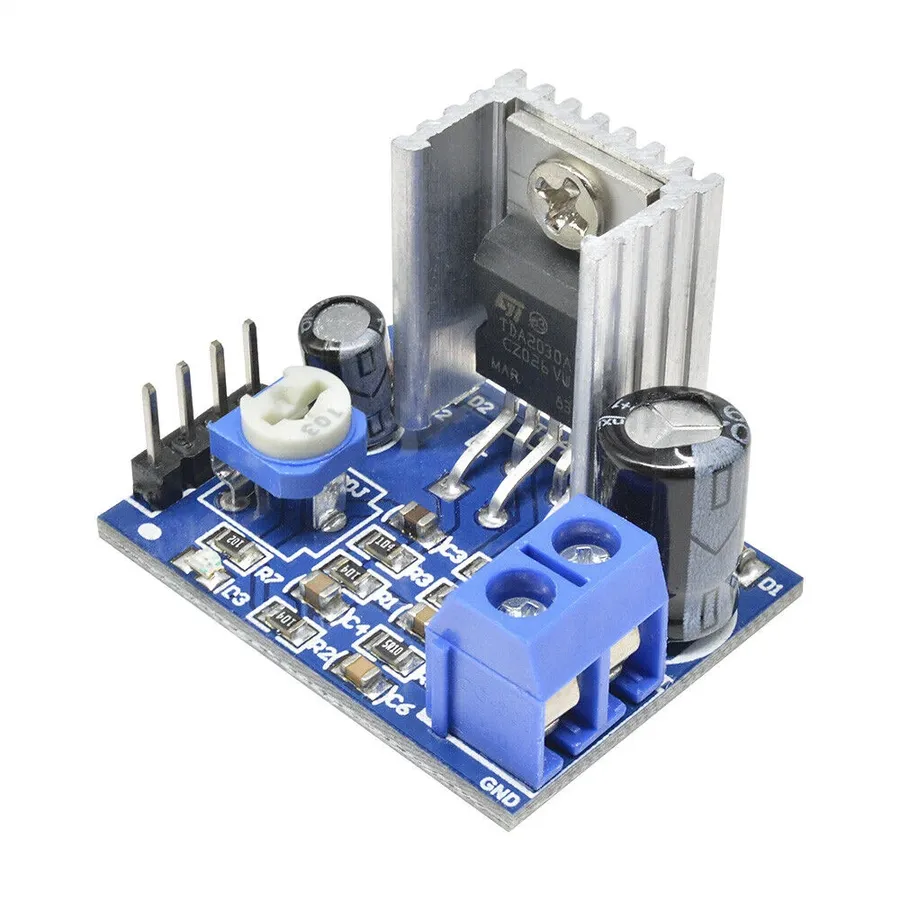
Creating a stereo amplifier with the TDA2030 integrated circuit involves using two identical amplifier circuits, one for the left channel and one for the right channel, to deliver full-range audio with enhanced fidelity. This configuration leverages the TDA2030's ability to provide a robust power output while maintaining a relatively simple design, making it ideal for DIY audio enthusiasts aiming for a hi-fi experience.
To construct a stereo amplifier, two TDA2030 ICs are required, along with associated passive components to support each channel. A common configuration involves splitting the incoming stereo audio signal and feeding each signal into the respective amplifier circuit. Furthermore, careful attention should be paid to the power supply, as it needs to provide enough current to both TDA2030 ICs simultaneously. To ensure optimal performance and minimize potential issues, it is recommended to use a well-regulated power supply and provide sufficient heatsinking for each TDA2030 IC.
| Component | Purpose | Typical Value (Per Channel) |
|---|---|---|
| TDA2030 IC | Audio Power Amplifier | 1 |
| Input Capacitor | Blocking DC Component | 1-10 µF |
| Feedback Resistor | Gain Setting | 22 kΩ - 47 kΩ |
| Ground Resistor | Gain Setting and Stability | 1 Ω - 2.2 Ω |
| Output Capacitor | Output DC Blocking | 220-1000 µF |
| Power Supply Capacitor | Bypass & Power Smoothing | 100-1000 µF |
| Heatsink | Thermal Dissipation | Adequate for Heat Load |
Optimizing a TDA2030 amplifier circuit involves careful component selection and circuit design to achieve the best possible audio quality. This includes minimizing distortion, reducing noise, and shaping the frequency response to meet specific application requirements. These enhancements are crucial for achieving a high-fidelity audio experience.
Key techniques for optimization revolve around power supply decoupling, feedback network design, and input stage configuration. Proper component selection, such as low-noise resistors and capacitors, also plays a crucial role in enhancing the TDA2030’s performance.
| Optimization Area | Technique | Impact |
|---|---|---|
| Distortion Reduction | Careful selection of feedback components, ensuring operation within the safe operating area | Improved audio clarity and reduced signal artifacts |
| Noise Minimization | Power supply decoupling, low-noise component selection, optimized circuit layout | Lower background noise, cleaner signal |
| Frequency Response Shaping | Adjusting feedback components and adding external filters | Tailored response for different audio applications |
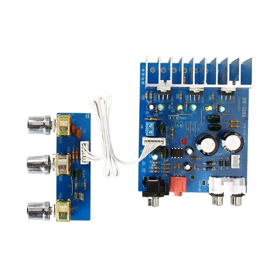
Designing a TDA2030-based subwoofer amplifier requires careful attention to low-frequency response and power delivery. This section details the specific design considerations for achieving optimal bass performance, including filtering techniques and adequate power supply to drive the subwoofer effectively.
Key to designing a TDA2030 subwoofer amplifier is the implementation of a low-pass filter, ensuring only low frequencies are amplified. This prevents the amplification of mid and high frequencies, which would otherwise muddy the bass. The cutoff frequency of the low-pass filter must be chosen based on the intended subwoofer's operational frequency range.
Power requirements for a subwoofer amplifier typically exceed those of a full-range speaker amplifier. The TDA2030, when used in a bridged configuration, can supply greater power output to drive the subwoofer. Sufficient heatsinking is critical to manage the power dissipation during the amplification of high-amplitude, low-frequency signals. Moreover, an adequate power supply, both in terms of voltage and current capability, should be employed to satisfy the amplifier’s requirements, particularly during peak output.
Components selection plays a critical role in the subwoofer amplifier design. High-quality capacitors should be used in the signal path to minimize signal loss and distortion. Additionally, the choice of the inductor for the low-pass filter can affect the Q factor of the filter and consequently the overall sound of the low end. Detailed circuit diagrams, including component values, are imperative for an effective build.
This section addresses common questions regarding the TDA2030 amplifier circuit, providing concise, practical answers for both novice and experienced users. We'll cover critical aspects like voltage limits, implementation, alternative ICs, and power output capabilities, ensuring a comprehensive understanding for your audio projects.
Building with the TDA2030 amplifier can sometimes present challenges. This section focuses on common issues encountered and provides systematic troubleshooting steps to help you achieve the desired performance.
The TDA2030 amplifier circuit provides an excellent foundation for building high-quality audio amplifiers. By understanding its core principles, experimenting with various circuit designs, and optimizing your implementations, you can unlock its full potential and create an audio system that meets your unique requirements. Just as a finely crafted musical instrument creates beautiful sounds, your understanding of the TDA2030 will lead to powerful audio experiences. The journey to mastering audio amplification begins with this circuit, and your continued experimentation and dedication will allow you to fine-tune the performance to your taste.

