AnyPCBA PCB and PCBA case studies


Our client, a manufacturer of compact electronic devices for consumer and industrial applications, needed a reliable, high-density interconnect (HDI) PCB that could support complex routing in a limited board space. The design required a standard HDI structure with fine lines and precise mechanical drilling to meet performance and cost targets.
Key Manufacturing Challenges:
HDI Structure: 6-layer board with 1+4+1 HDI build-up architecture
Fine Lines: 4/4mil line width and spacing for dense routing
Precision Drilling: 0.1mm minimum mechanical hole size
Surface Finish: ENIG for excellent solderability and oxidation resistance
Cost-Effective Production: Manufacturable design for medium-volume production
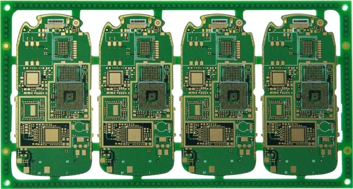
AnyPCBA provided comprehensive PCB fabrication services for this HDI board, from engineering review to final electrical testing.
Our manufacturing approach included:
HDI Process Engineering: Optimized the 1+4+1 sequential lamination process for the 6-layer structure
Fine Line Etching: Controlled etching process to achieve 4/4mil line width/spacing with high yield
Precision Drilling: High-accuracy mechanical drilling for 0.1mm holes
Impedance Control: Carefully designed stack-up to meet impedance specifications
Surface Finish: ENIG (Electroless Nickel Immersion Gold) for flat, oxidation-resistant pads
Cost Optimization: Design for manufacturability to ensure cost-effective medium-volume production
Rigorous Testing: Comprehensive electrical testing to ensure reliability
| Parameter | Specification |
|---|---|
| Layer Count | 6 layers |
| HDI Structure | 1+4+1 (sequential lamination) |
| Board Thickness | 1.0mm |
| Minimum Line Width/Space | 4/4mil |
| Minimum Mechanical Hole | 0.1mm |
| Surface Finish | ENIG (Electroless Nickel Immersion Gold) |
| Application | Compact consumer and industrial electronics |
Successful Fabrication: Delivered high-quality 6-layer 1+4+1 HDI PCBs meeting all specifications
Standard HDI Capability: Demonstrated reliable manufacturing for widely-used HDI structures
Fine Line Expertise: Achieved 4/4mil line width/spacing with consistent quality
Cost-Effective Solution: Optimized design for manufacturability and production efficiency
Reliable Quality: ENIG surface finish and rigorous testing ensured field reliability
Versatile Manufacturing: Proven capability for a wide range of HDI applications
This case demonstrates AnyPCBA's capability to handle standard HDI PCB fabrication challenges for consumer and industrial electronics:
✅ Standard HDI structures (6-layer, 1+4+1 sequential lamination)
✅ Fine lines (4/4mil line width/spacing)
✅ Precision mechanical drilling (0.1mm holes)
✅ Reliable surface finish (ENIG)
✅ Cost-effective production (medium-volume capable)
Ready to discuss your HDI PCB or compact design project? Contact us to learn how AnyPCBA can support your PCB fabrication needs.