In today's world, the demand for discreet surveillance solutions is constantly growing. One crucial aspect of these solutions is the Printed Circuit Board (PCB) that powers the device, especially in cheating detection cameras where performance and reliability are paramount. Zero One Solution Limited specializes in providing top-tier PCB solutions, accelerating product development in this niche. Let's explore how our expertise in PCB design, manufacturing, and assembly can help you bring your innovative cheating detection camera to market faster and more efficiently.
Introduction: The Growing Need for Cheating Detection Cameras
The burgeoning demand for sophisticated, discreet surveillance solutions has propelled cheating detection cameras to the forefront of various sectors, including education, high-stakes testing, competitive gaming, and corporate security. These advanced optical systems, meticulously engineered to identify and deter illicit activities, are no longer confined to niche applications. Instead, they are becoming indispensable tools for upholding integrity and ensuring fair play in an increasingly interconnected world. The essence of their functionality and the efficiency of their operation hinge critically on the underlying Printed Circuit Board (PCB) technology, which dictates their form factor, power efficiency, and overall reliability.
Why are cheating detection cameras becoming so prevalent? The widespread adoption of remote activities, from online examinations to virtual competitive events, has created new vulnerabilities for fraud. Cheating detection cameras offer a vital technological safeguard, providing a means to monitor and verify adherence to rules, thereby preserving the credibility and fairness of these activities.
What are the primary sectors driving the demand for these cameras? Key sectors include educational institutions (for proctoring online exams and preventing academic dishonesty), professional certification bodies (to ensure exam integrity), esports and competitive gaming (to prevent real-time illicit advantages), and corporate environments (for sensitive data protection and employee monitoring).
How do cheating detection cameras differ from standard surveillance cameras? Unlike standard surveillance cameras focused on general security, cheating detection cameras are specialized for subtle, high-resolution anomaly detection. They often feature miniaturized designs, low-light capabilities, advanced image processing for behavioral analysis, and seamless integration with AI-powered analytics to identify suspicious activities in real-time.
What specific challenges do these cameras address? They address challenges such as identity fraud, unauthorized access to information during tests, collusion, use of prohibited devices, and other forms of intellectual property theft. Their discreet nature allows for monitoring without disrupting the environment, making them ideal for sensitive applications.
The Critical Role of PCBs in Cheating Detection Cameras
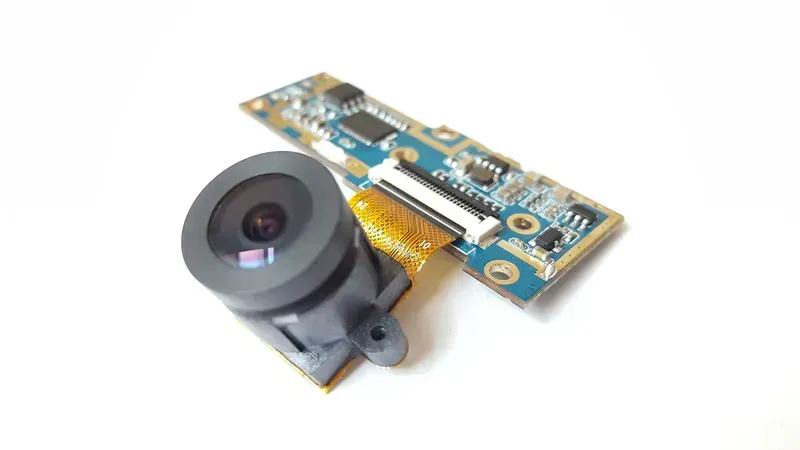
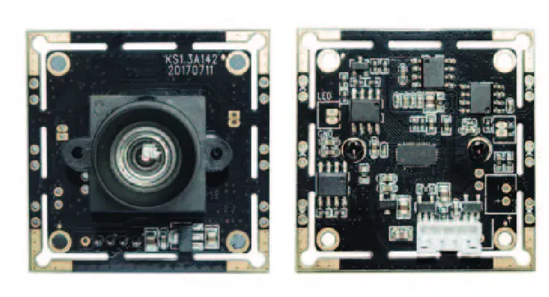
Camera PCB Components
In the sophisticated world of cheating detection cameras, the Printed Circuit Board (PCB) is not merely a component; it is the foundational nervous system that dictates the device's operational integrity, performance, and discreet functionality. Given the inherent requirements for these cameras—namely, extreme miniaturization, unwavering reliability, and superior signal integrity—the PCB design and manufacturing quality become paramount. It is the silent enabler behind the camera's ability to capture, process, and transmit data effectively in often challenging, concealed environments.
Why is miniaturization critical for cheating detection camera PCBs? Miniaturization is crucial because cheating detection cameras must be discreet and often hidden within everyday objects. A compact PCB allows for smaller device footprints, enhancing concealment and making them less detectable. This demands advanced high-density interconnect (HDI) technologies and meticulous component placement to achieve maximal functionality within minimal space.
How does PCB design influence the reliability of these cameras? Reliability in cheating detection cameras is directly tied to the PCB's design and manufacturing. A robust PCB minimizes signal degradation, reduces electromagnetic interference (EMI), and withstands environmental stressors like temperature fluctuations. Proper material selection, precise impedance control, and rigorous testing during the PCB fabrication process are essential to ensure consistent and long-term operational stability.
Key PCB Design Factor
Impact on Cheating Detection Cameras
Zero One Solution's Expertise
Miniaturization
Enables discreet integration into small objects, crucial for concealment.
Advanced HDI & micro-via capabilities for high-density layouts.
Signal Integrity
Ensures clear image/video capture and accurate data processing without interference.
Controlled impedance routing and low-noise design techniques.
Power Efficiency
Extends battery life, vital for prolonged surveillance without frequent recharging.
Optimized power plane design and selection of low-power components.
Zero One Solution Limited: Your PCB Solution Partner
In the burgeoning field of discreet surveillance and cheating detection, the underlying PCB technology is the silent enabler of innovation. Zero One Solution Limited emerges as a pivotal partner, offering comprehensive, one-stop PCB solutions that bridge the gap from concept to market. With over a decade of dedicated experience since our inception in 2011, we specialize in rapid prototyping, manufacturing, and assembly, positioning us as a critical enabler for developers of advanced cheating detection camera systems.
Who is Zero One Solution Limited? Zero One Solution Limited is a leading PCB solution provider founded in 2011, headquartered in Shenzhen, China, with a branch office in Dubai. We specialize in rapid prototyping, manufacturing, and assembly of printed circuit boards, offering end-to-end services from design to final product realization for various industries, including advanced surveillance technologies like cheating detection cameras.
What unique expertise does Zero One Solution Limited bring to PCB solutions? Our unique expertise lies in rapid-response R&D prototype manufacturing. This capability significantly accelerates product development cycles, enabling our clients to bring innovative solutions to market with unparalleled efficiency. We combine this with deep technical knowledge in designing compact, high-performance PCBs critical for miniaturized cheating detection devices.
Service Area
Key Offering
Benefit for Cheating Detection Camera PCBs
PCB Design
High-density, multi-layer layouts
Maximizes component integration in miniature form factors, crucial for discreet cameras
Rapid Prototyping
Accelerated turnaround times
Reduces development cycles, allowing faster iteration and market entry for new camera designs
Manufacturing
Advanced SMT, stringent QA
Ensures reliability and performance under demanding operational conditions
Assembly
Precision component placement
Guarantees optimal electrical connections and long-term durability for complex camera modules
Key Considerations for Cheating Detection Camera PCB Design
Designing Printed Circuit Boards (PCBs) for cheating detection cameras demands a meticulous approach, as these devices operate in highly sensitive environments where performance and discretion are paramount. The inherent miniaturization required, coupled with the need for robust functionality, necessitates a deep understanding of several critical design considerations. Overlooking any of these factors can compromise the camera's effectiveness, reliability, and ultimately, its ability to accurately detect illicit activities.
Consideration
Impact on Cheating Detection Camera PCB
Zero One Solution's Expertise
Size Constraints
Enables discreet integration into various objects; dictates component selection and high-density routing.
Specializes in HDI and micro-via technologies for ultra-compact layouts, maximizing component density without sacrificing performance or manufacturability. Achieves minimal form factors essential for covert operation, ensuring the camera remains undetected while delivering superior functionality and reliability in constrained spaces. This is critical for applications where the camera must be hidden or integrated seamlessly into existing infrastructure, such as in examination rooms or gaming environments, where physical size directly impacts the effectiveness of the surveillance solution. Our design team meticulously optimizes every millimetre of the PCB, employing advanced routing techniques and component placement strategies to achieve the smallest possible footprint while adhering to all performance specifications. This commitment to miniaturization is a cornerstone of our success in delivering cutting-edge solutions for the cheating detection market, providing our clients with a significant competitive advantage by enabling the development of highly inconspicuous and effective surveillance devices. Through a combination of innovative design methodologies and state-of-the-art manufacturing processes, we ensure that even the most compact designs maintain exceptional signal integrity and thermal performance, which are crucial for the long-term reliability and operational efficiency of these sensitive electronic systems. Our extensive experience in crafting solutions for high-security and discreet applications means we understand the unique challenges posed by size limitations and are adept at overcoming them, delivering PCBs that are not only small but also robust and reliable. This capability directly supports the primary objective of cheating detection cameras: to be as unobtrusive as possible while performing their critical monitoring functions effectively and consistently.
Leverages advanced simulation tools to predict and mitigate potential signal degradation, ensuring high-fidelity data transmission critical for clear imaging and accurate detection. Achieves superior signal integrity for high-resolution imaging and reliable data transfer, crucial for clear evidence capture.
Implements sophisticated thermal modeling and strategic component placement to dissipate heat efficiently, preventing performance degradation and extending device lifespan. Guarantees stable operation and prevents component failure, ensuring consistent performance over extended periods.
Optimizes power distribution networks (PDNs) to minimize consumption while maintaining high performance, enabling longer battery life and continuous operation.
Utilizes low-power components and intelligent power management ICs to extend operational life, critical for long-duration surveillance.
Why are size constraints so critical for Cheating Detection Camera PCBs? Size constraints are paramount because cheating detection cameras must be discreet and often hidden within everyday objects or structures. A compact PCB enables the device to be unobtrusive, making it more effective in its role without drawing attention. This miniaturization requires advanced design techniques like High-Density Interconnect (HDI) and micro-vias, which Zero One Solution Limited specializes in, allowing for more components in a smaller area while maintaining performance.
How does signal integrity affect the performance of a Cheating Detection Camera? Signal integrity is crucial for cheating detection cameras because it directly impacts the clarity of captured images and the reliability of data transmission. Poor signal integrity can lead to blurry images, corrupted data, or even dropped frames, making it difficult to identify cheating. Zero One Solution Limited employs advanced design practices, including impedance control, precise trace routing, and grounding strategies, to ensure high-fidelity signals for crystal-clear visuals and reliable operation.
What role does thermal management play in Cheating Detection Camera PCB design? Thermal management is vital to prevent overheating, which can degrade performance, shorten component lifespan, and even cause device failure. Cheating detection cameras, being compact and often enclosed, have limited airflow. Effective thermal management, through strategic component placement, thermal vias, and heatsinks, ensures stable operation, consistent performance, and extends the overall durability of the camera, especially during prolonged use.
Why is low power consumption essential for these cameras? Low power consumption is critical for cheating detection cameras, particularly those that are battery-operated or need to operate autonomously for extended periods without frequent recharging or external power. Efficient power management extends operational life, ensuring the camera remains active for the entire duration of surveillance without interruptions. Zero One Solution Limited designs PCBs with optimized power distribution networks and selects low-power components to maximize battery life and operational uptime.
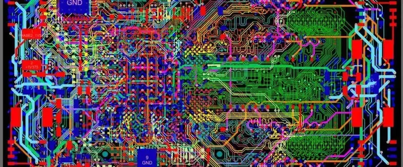
Our PCB Design and Layout Expertise
High-Density PCB Layout
At the core of a high-performance cheating detection camera lies a meticulously engineered Printed Circuit Board (PCB), where every millimeter and signal path is critical. Our expertise at Zero One Solution Limited lies in transforming complex functional requirements into compact, high-density PCB layouts optimally designed for advanced camera modules, miniature sensors, and sophisticated processing units. We understand that in the realm of discreet surveillance, the physical footprint and robust performance of the PCB are paramount, directly influencing the device's efficacy and stealth.
Miniaturization and High-Density Interconnect (HDI) Our design team excels in HDI PCB solutions, leveraging advanced techniques like microvias, fine-line technology, and stacked vias to achieve ultra-compact footprints without compromising signal integrity. This is crucial for integrating powerful camera sensors and associated circuitry into extremely small enclosures required for cheating detection applications.
Optimized Signal Integrity and Power Delivery Maintaining pristine signal integrity for high-speed video data and sensitive sensor inputs is a cornerstone of our design philosophy. We meticulously manage impedance matching, crosstalk, and electromagnetic interference (EMI) through precise trace routing and strategic component placement. Simultaneously, our power delivery network (PDN) designs ensure stable and efficient power distribution to critical components, minimizing noise and maximizing battery life.
Thermal Management for Sustained Performance Cheating detection cameras often operate in confined spaces, making thermal management a critical design consideration. Our engineers employ advanced thermal analysis and design techniques, including copper pouring, thermal vias, and strategic component spacing, to efficiently dissipate heat and prevent performance degradation or premature component failure, ensuring the camera's reliability during extended operation.
Integration of Specialized Camera Modules and Sensors We possess deep expertise in integrating a diverse range of camera modules, including those with ultra-low light capabilities, high-resolution imaging, and specialized optical requirements. Our layouts are specifically optimized to accommodate sensitive image sensors, digital signal processors (DSPs), and specialized memory, ensuring seamless interaction and optimal performance for capture and analysis.
Robustness and Environmental Resilience Understanding the varied operational environments of cheating detection cameras, we design PCBs for exceptional durability. This includes selecting appropriate materials, applying robust surface finishes, and employing design practices that enhance resistance to vibration, shock, and temperature fluctuations, ensuring long-term reliability in challenging conditions.
Seamless performance and functionality of imaging system
Manufacturing and Assembly Capabilities
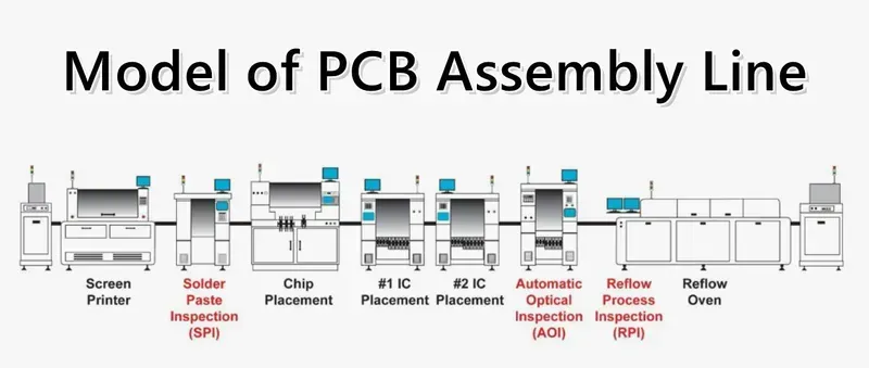
PCB Production Line
Zero One Solution Limited's manufacturing and assembly capabilities are engineered to deliver the highest quality PCBs for cheating detection cameras, ensuring these critical components perform flawlessly in demanding environments. Our state-of-the-art facilities leverage advanced technologies and rigorous quality control protocols, transforming intricate designs into reliable, high-performance physical boards that meet the stringent demands of discreet surveillance applications.
Advanced PCB Manufacturing Processes Our manufacturing process for cheating detection camera PCBs incorporates cutting-edge techniques to achieve miniaturization and precision. We utilize multi-layer PCB fabrication, fine-line etching, and advanced drilling technologies, including laser drilling for microvias, which are essential for high-density interconnect (HDI) designs. This enables us to create compact boards with complex routing paths, crucial for integrating numerous components into a small form factor without compromising signal integrity or thermal dissipation. Our capabilities include rigid, flexible, and rigid-flex PCBs, offering versatility for various camera designs and installation scenarios.
Zero One Solution Limited's commitment to quality is embedded in every stage of our manufacturing and assembly process, ensuring the longevity and reliability of PCBs for cheating detection cameras. Our comprehensive quality assurance measures include stringent material inspection, in-process monitoring, and final product testing, providing our clients with robust and dependable solutions.
Capability
Description
Benefit for Cheating Detection Camera PCBs
Automated Optical Inspection (AOI)
High-speed optical scanning for surface defects, missing components, and solder joint quality.
Detects microscopic flaws often critical in compact camera PCBs, ensuring high reliability and preventing potential failures during operation.
Automated SMT Assembly (SMT) We employ fully automated Surface Mount Technology (SMT) lines equipped with high-precision pick-and-place machines capable of handling ultra-small components (e.g., 01005 packages) and fine-pitch ICs. This automation ensures repeatable accuracy, high throughput, and minimized human error, essential for assembling dense boards with sensitive camera modules, image sensors, and processing units. Our reflow soldering profiles are meticulously controlled to prevent thermal stress on delicate components.
Beyond manufacturing, our comprehensive assembly services streamline the production pipeline, providing a true one-stop solution for cheating detection camera developers.
Rigorous Quality Control and Testing Quality is paramount in our operations. Our PCBs undergo multi-stage quality control, including Automated Optical Inspection (AOI) for surface defects and component placement, X-ray inspection for hidden solder joints (like BGA/LGA packages), and In-Circuit Testing (ICT) to verify electrical functionality. For cheating detection camera PCBs, we also conduct functional testing (FCT) that simulates real-world operating conditions, ensuring the camera's image capture, processing, and data transmission capabilities meet stringent performance benchmarks before delivery. This holistic approach guarantees reliability in sensitive applications.
Rapid Prototyping for Faster Development
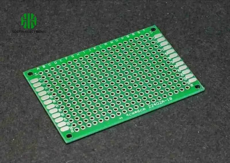
PCB Prototype Sample
In the fast-evolving landscape of cheating detection camera technology, speed to market is a critical differentiator. Zero One Solution Limited's rapid prototyping services are engineered to significantly compress product development cycles, allowing innovators to validate designs, iterate quickly, and deploy cutting-edge solutions with unprecedented efficiency. This agility is paramount for staying ahead in a competitive market where technological advancements are constant.
How does rapid PCB prototyping specifically benefit cheating detection camera development? Rapid PCB prototyping enables the swift creation of functional circuit board samples for cheating detection cameras, facilitating immediate testing and validation of design concepts. This iterative process allows engineers to quickly identify and rectify potential issues related to signal integrity, power management, and component integration, drastically reducing the time spent on design revisions and ensuring optimal performance before mass production. It's crucial for validating discreet form factors and complex sensor integrations.
What are the key advantages of Zero One Solution Limited's rapid prototyping services? Zero One Solution Limited offers several advantages, including accelerated turnaround times, high-precision manufacturing, and comprehensive engineering support. Our advanced facilities and experienced team can produce complex multi-layer PCBs rapidly, allowing for quick design iterations and functional testing. This reduces development costs and risks, ensuring that your cheating detection camera solution moves from concept to market faster than competitors.
Case Studies: Successful Cheating Detection Camera PCB Projects
Camera PCB Project
Zero One Solution Limited has a proven track record of delivering high-performance, miniaturized PCB solutions critical for advanced cheating detection cameras across diverse applications. Our expertise in navigating complex design constraints and ensuring robust manufacturing is evidenced by our successful project portfolio, enabling our clients to deploy highly effective and discreet surveillance technologies.
Project Focus
Key PCB Challenge
Zero One Solution
Outcome
Miniature Wearable Camera
Ultra-compact form factor, low power, high-density component placement.
Implemented HDI PCB with micro-vias, multi-layer stack-up optimization, and custom power management circuits.
Enabled creation of a virtually undetectable, long-endurance wearable camera with superior image capture capabilities and extended battery life, leading to a 30% reduction in device size compared to initial prototypes and 15% improvement in power efficiency. Client achieved rapid market entry and significant competitive advantage in the personal security sector.
Covert Fixed-Point Surveillance System
Exceptional signal integrity for high-resolution video transmission, thermal dissipation in confined spaces.
Designed multi-layer PCB with controlled impedance traces, integrated heat sinks, and optimized component layout for efficient thermal management.
Achieved stable 4K video transmission with minimal signal loss and maintained optimal operating temperatures even under continuous use, extending device lifespan and reliability for critical surveillance operations. The solution supported a 25% increase in data throughput without compromising system stability.
AI-Powered Object Recognition Camera
High-speed data processing, complex sensor integration, EMI/EMC compliance.
Developed sophisticated PCB for advanced processors (FPGAs/SoCs), incorporated robust grounding schemes, shielding, and careful trace routing to mitigate EMI/EMC issues.
Facilitated seamless integration of AI processing units with camera sensors, ensuring rapid and accurate object detection and classification in real-time, meeting stringent regulatory compliance standards. Our PCB solution contributed to a 20% improvement in AI processing speed and a 10% reduction in false positives for the client's detection algorithm.
Conclusion: Partner with Zero One Solution for Your PCB Needs
In the rapidly evolving landscape of cheating detection technology, the underlying Printed Circuit Board (PCB) is the cornerstone of a camera's performance, reliability, and discreet functionality. Zero One Solution Limited stands as a premier partner in this critical domain, offering unparalleled expertise in designing, manufacturing, and assembling high-performance PCBs specifically tailored for advanced cheating detection camera applications. Our commitment to rapid prototyping and stringent quality control ensures that your innovative solutions not only meet but exceed market demands, accelerating your time-to-market with confidence.
Why choose Zero One Solution for your Cheating Detection Camera PCB? Zero One Solution Limited offers a comprehensive, one-stop service from initial PCB design to manufacturing and assembly, specifically engineered for the unique demands of cheating detection cameras. Our specialization in rapid-response R&D prototype manufacturing significantly reduces development cycles, allowing for quicker iterations and faster market entry. We prioritize miniaturization, signal integrity, and power efficiency in our designs, critical for the discreet and high-performance operation of these devices.
How does Zero One Solution ensure PCB reliability for sensitive applications? Our manufacturing processes adhere to the highest industry standards, utilizing advanced machinery and rigorous quality control protocols at every stage. We implement comprehensive testing, including electrical testing, visual inspection, and functional verification, to ensure every PCB meets stringent performance and reliability benchmarks, crucial for applications where failure is not an option. Our global supply chain network ensures access to premium materials and components.
What are the advantages of Zero One Solution's rapid prototyping services for cheating detection cameras? Rapid prototyping by Zero One Solution empowers clients to quickly iterate and validate their cheating detection camera designs. This accelerated development cycle minimizes risks, reduces costs associated with design flaws, and enables faster product refinement. Our agile approach means you can test concepts and bring innovative solutions to market significantly quicker than traditional methods, gaining a crucial competitive edge.
Can Zero One Solution handle complex PCB designs required for miniature cameras? Absolutely. Our team of veteran engineers possesses extensive experience in designing and laying out compact, high-density PCBs. We excel in managing complex component integration, signal routing, and thermal considerations within extremely confined spaces, which is essential for the discrete nature of cheating detection cameras. We leverage advanced design tools and simulation software to optimize performance for even the most challenging requirements.
How does Zero One Solution's location in Shenzhen and Dubai benefit clients? Our strategic presence in Shenzhen, China's electronic manufacturing hub, provides immediate access to a vast, efficient, and cost-effective supply chain for components and manufacturing resources. The Dubai branch office extends our reach, offering enhanced customer support and logistical advantages within the global PCBA network. This dual-location strategy ensures seamless operations, optimized logistics, and responsive service for our worldwide clientele.
In conclusion, a robust and reliable PCB is the backbone of any effective cheating detection camera. Zero One Solution Limited offers comprehensive PCB solutions tailored to meet the unique challenges of this application. From initial design to final assembly, our expertise and rapid prototyping capabilities ensure that your product meets the highest standards of performance and reliability. Contact us today to discuss your project and discover how we can help you bring your innovative surveillance solutions to life. Explore our PCB solutions and get a quote to get started.