Choosing ESA Qualified PCB Manufacturers: A Guide for Aerospace Excellence
2025.01.14
In the demanding realm of aerospace engineering, the reliability of every component is paramount. Printed Circuit Boards (PCBs) are at the heart of many critical systems, and selecting an ESA qualified PCB manufacturer is not merely a preference; it's a necessity for mission success. This article will guide you through the essential aspects of choosing the right ESA qualified PCB manufacturer, ensuring your project meets stringent quality and reliability standards, highlighting the importance of working with trusted partners like those certified by ESA.
Understanding ESA Qualification for PCBs
Aerospace PCB
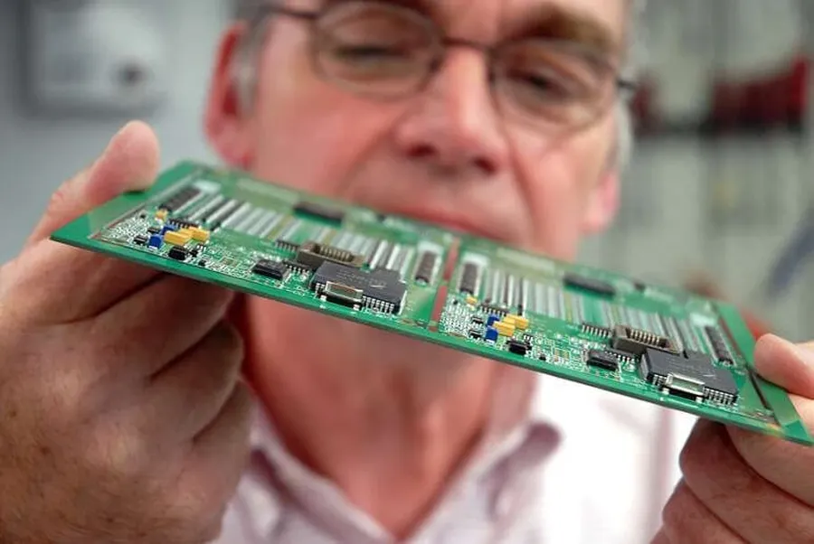
ESA qualification for Printed Circuit Board (PCB) manufacturers signifies adherence to stringent European Space Agency (ESA) standards, ensuring PCBs meet the rigorous demands of space and other high-reliability applications. This qualification is not merely a certification but a testament to a manufacturer's capability to produce PCBs that can withstand extreme conditions, including temperature fluctuations, radiation exposure, and mechanical stress, while maintaining optimal performance and reliability.
The core of ESA qualification lies in the ECSS (European Cooperation for Space Standardization) standards, notably ECSS-Q-ST-70-60C, which outlines the specific requirements for PCBs used in space missions. These standards mandate strict controls on materials, manufacturing processes, testing procedures, and overall quality management systems.
Achieving ESA qualification requires a PCB manufacturer to demonstrate consistent compliance with these demanding standards through comprehensive testing and audits. The benefits of using ESA-qualified PCBs include enhanced reliability, reduced risk of failure in critical missions, and assurance of long-term performance in harsh operational environments.
Key Standards and Requirements for ESA Qualified PCBs
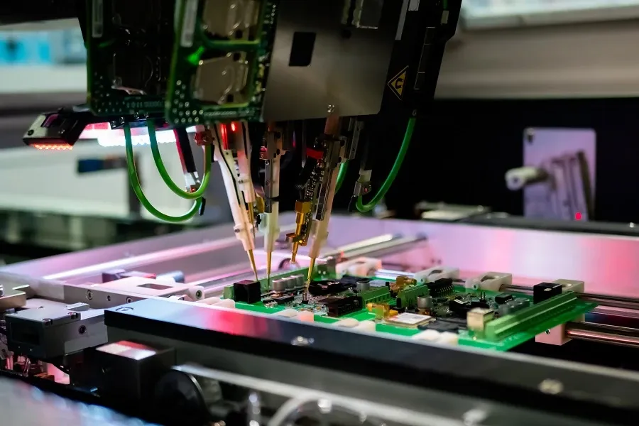
PCB Testing Equipment
ESA-qualified PCB manufacturers must adhere to stringent technical requirements and quality standards, primarily defined by the European Cooperation for Space Standardization (ECSS). These standards ensure the reliability and performance of PCBs in harsh space environments, focusing on material selection, manufacturing processes, and rigorous testing protocols.
Standard Area
Specific Requirements
Key ECSS Standards
Material Selection
Use of approved materials that can withstand extreme temperatures, radiation, and vacuum conditions. Controlled outgassing properties are crucial to prevent contamination.
ECSS-Q-ST-70-02, ECSS-Q-ST-70-08, ECSS-Q-ST-70-12
Manufacturing Processes
Precise control over all manufacturing steps, including etching, drilling, plating, and lamination to ensure dimensional accuracy and consistent electrical performance. Traceability of process parameters is essential.
ECSS-Q-ST-70-10, ECSS-Q-ST-70-12
Environmental Testing
Rigorous environmental testing, such as thermal cycling, vibration, shock, and vacuum tests, are conducted to verify the PCB's reliability in space environments. These tests simulate the stresses encountered during launch and operation.
ECSS-Q-ST-70-06, ECSS-Q-ST-70-60C
Quality Management
A robust quality management system that conforms to ECSS requirements is mandatory. This includes document control, process validation, and regular audits.
ECSS-Q-ST-10, ECSS-Q-ST-70
The most relevant ECSS standards include ECSS-Q-ST-70-02 for material selection and control, ECSS-Q-ST-70-10 for PCB manufacturing processes and quality management, and ECSS-Q-ST-70-60C for the qualification and acceptance of PCBs for space applications. Adherence to these standards is critical for ensuring the PCBs meet the demanding performance and reliability requirements of space missions.
Identifying ESA Qualified PCB Manufacturers
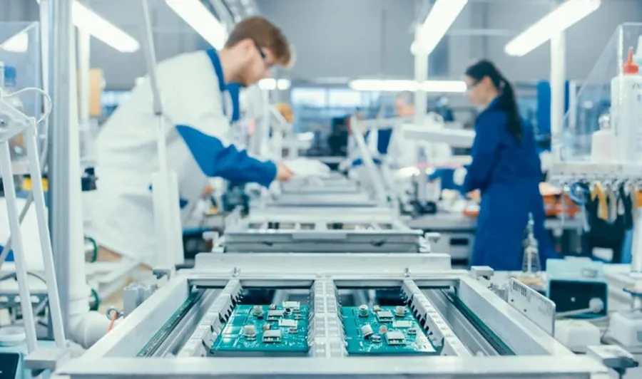
PCB Factory
Locating ESA-qualified PCB manufacturers requires accessing specialized resources and directories, primarily the ESCIES (European Space Components Information Exchange System) website. This section outlines how to effectively identify these manufacturers, understand the types of certifications, and their implications for your project, ensuring that your PCBs meet the stringent demands of space and high-reliability applications.
Utilize the ESCIES Database The ESCIES website is the primary resource for identifying ESA-qualified manufacturers. Search their database, which often includes a list of manufacturers certified to produce PCBs compliant with ECSS standards, including ECSS-Q-ST-70-60C. This database is continuously updated, ensuring access to current certifications.
Verify Manufacturer Certifications ESA qualification isn't a singular, blanket certification. Manufacturers can be certified to different levels and standards within the ECSS framework. It is crucial to verify that the manufacturer possesses certification that matches your specific project requirements. For instance, a manufacturer might be certified for space applications under the ECSS-Q-ST-70-12C but not the more stringent ECSS-Q-ST-70-60C, or vice versa.
Review Product Specific Approvals Confirm that the manufacturer's certification covers the specific PCB technologies and materials needed for your project. Some manufacturers may hold ESA certification for standard PCBs, but not for high-density interconnect (HDI) PCBs, or they may have limited approvals for specific materials. This verification is crucial to ensure the final product meets performance and reliability needs.
Cross-Reference with Other Industry Directories While ESCIES is the primary resource, it is beneficial to cross-reference information with other industry directories or relevant databases that may list manufacturers specializing in high-reliability or aerospace PCBs. This adds a layer of verification and could uncover manufacturers that are not yet listed in the ESCIES.
Engage Directly with Manufacturers After identifying potential manufacturers through directories, directly contact them to discuss your specific requirements. Request copies of their certification documents, ask for details about their manufacturing processes, and ensure they have experience producing PCBs for your application's demands. Direct engagement is essential for proper assessment.
The Role of Material Certification in ESA Qualification
PCB Material Samples
Material certification is a cornerstone of the ESA qualification process for PCB manufacturers, ensuring that the materials used in printed circuit boards meet stringent performance and reliability standards crucial for space applications. The selection of appropriate materials is not arbitrary; it's dictated by the extreme conditions PCBs will face, demanding a thorough understanding of how these materials behave under stress, radiation, and thermal variations.
The European Cooperation for Space Standardization (ECSS) standards, particularly ECSS-Q-ST-70-60C, specify the requirements for materials used in space hardware. These standards cover a broad range of material properties, including thermal stability, outgassing behavior, and resistance to radiation. Manufacturers must demonstrate that their chosen materials not only meet the minimum requirements, but also maintain their integrity and performance throughout the mission life of the application.
Material Property
Importance in Space Applications
ECSS Standard Focus
Thermal Stability
Maintains performance over extreme temperature ranges.
ECSS-Q-ST-70-60C emphasizes limits on thermal expansion and degradation.
Outgassing
Prevents contamination of sensitive space instruments.
ECSS-Q-ST-70-02 defines acceptable levels of outgassing for non-metallic materials.
Radiation Resistance
Ensures material functionality after long exposure to space radiation.
Specific ECSS standards outline radiation testing and performance requirements.
Mechanical Strength
Maintains structural integrity under vibration and shock
Relevant ECSS mechanical standards outline testing and qualification requirements.
For example, materials like Ventec VT-901 are often specified for space-grade PCBs due to their low outgassing properties, high thermal stability, and proven performance in harsh environments. ESA approval for specific materials involves extensive testing and documentation, confirming compliance with relevant ECSS standards. The selection process needs to be rigorous, since the performance of the materials directly translates to the overall mission success.
HDI Technology and ESA Qualification
HDI PCB
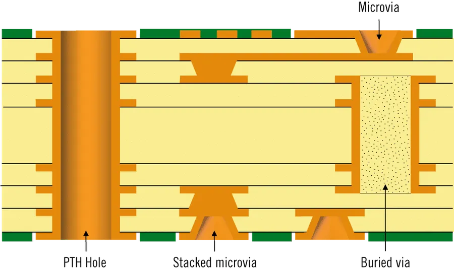
High-Density Interconnect (HDI) technology is increasingly vital in space applications, driven by the need for smaller, lighter, and more capable electronic systems. Achieving ESA qualification for HDI PCBs ensures these advanced interconnect solutions meet stringent reliability and performance standards required for space missions.
The escalating demand for HDI PCBs in aerospace stems from their ability to accommodate complex circuitry within a reduced footprint. This density advantage, coupled with enhanced electrical performance, makes HDI technology indispensable for contemporary space electronics. Therefore, understanding how manufacturers achieve ESA qualification for HDI PCBs is vital for the selection process.
ESA qualification for HDI PCBs is not simply a matter of applying the same standards as traditional PCBs. The miniaturization and enhanced complexity of HDI require stringent control over materials, fabrication processes and testing regimes.
Manufacturers seeking ESA qualification for HDI PCBs must demonstrate adherence to ECSS standards, particularly concerning material selection, plating processes, and microvia formation. These standards ensure that HDI PCBs withstand the severe thermal, mechanical, and radiation environments encountered in space.
Key aspects of the qualification process include rigorous testing of microvia reliability, ensuring structural integrity of the thin dielectrics used, and verification of long-term solder joint reliability, especially under thermal cycling.
The significance of ESA qualification for HDI PCBs is paramount in ensuring that these advanced interconnect solutions perform reliably in the harsh environment of space. This qualification offers assurance of consistent quality, durability, and performance, aligning with the stringent requirements of space missions and contributes significantly to mission success.
Navigating the Procurement Process for ESA Qualified PCBs
PCB Inspection
Procuring ESA-qualified PCBs requires a meticulous approach to ensure the highest reliability and compliance with stringent aerospace standards. This process involves careful vendor selection, detailed specification reviews, thorough documentation management, and rigorous quality audits. The goal is to mitigate risks associated with component failure in critical applications by partnering with manufacturers who demonstrate a proven commitment to ESA requirements.
Initial Supplier Qualification Begin by thoroughly vetting potential manufacturers. Look for certifications, experience in producing ESA-qualified PCBs, and a demonstrated understanding of ECSS standards (e.g., ECSS-Q-ST-70-60C). Verification of their quality management system is essential.
Detailed Technical Specification Review Ensure that your PCB specifications are comprehensively defined and align with the selected manufacturer’s capabilities. This includes materials, layer stack-up, tolerances, and specific performance requirements, clearly communicate and confirm these specifications with the manufacturer.
Material Traceability and Certification Request and verify material certifications. Materials like Ventec VT-901 have specific ESA approvals, and traceability must be maintained throughout the manufacturing process. Ensure that the manufacturer can supply batch-specific certifications.
Comprehensive Documentation Requirements Establish clear documentation requirements, including manufacturing process flows, test reports, and certificates of conformity. All documentation should comply with relevant ECSS standards.
Regular Audits and Inspections Plan and conduct regular audits of the manufacturing facility to verify compliance and adherence to specified processes. The frequency and scope of these audits should be defined based on the criticality of the PCB application.
Risk Management and Mitigation Implement a comprehensive risk management plan, identifying potential issues and establishing mitigation strategies. This includes contingency plans for production delays or material shortages.
Ongoing Communication and Collaboration Maintain open lines of communication with the manufacturer. Regular progress updates and collaboration are crucial for ensuring quality and addressing issues that may arise during the manufacturing process.
Procurement Phase
Key Activities
Expected Outcome
Pre-Procurement
Identify potential ESA-qualified manufacturers, check certifications, review past performance.
A qualified shortlist of suppliers is developed.
Specification Definition
Detail PCB specifications and ensure alignment with ECSS standards, verify the supplier's capabilities
Clear, technically sound specifications are finalized.
Quotation and Review
Gather and analyze quotations. verify material certifications and traceability.
Cost-effective, compliant quote from a qualified supplier
Contract and Documentation
Establish clear terms of supply, delivery requirements, audit procedures and documentation.
Signed contract that covers all critical aspects.
Production Monitoring
Regular audits of production, monitoring quality metrics and progress reports.
Production is done as specified and on schedule.
Final Delivery and Review
Thorough review of documentation and delivered products before accepting delivery
Complete set of documentation and compliant PCBs delivered
Frequently Asked Questions about ESA Qualified PCBs
This section addresses common inquiries regarding ESA qualified PCBs, focusing on cost, lead times, certification levels, and other critical factors to help you make informed decisions.
What does 'ESA qualified' mean for a PCB manufacturer? An ESA qualified PCB manufacturer has demonstrated compliance with the European Space Agency's stringent requirements for producing printed circuit boards suitable for space applications. This involves adherence to specific standards, rigorous testing, and quality assurance processes, often detailed in the ECSS standards.
What are the key ECSS standards for ESA qualified PCBs? The primary ECSS standards related to PCB qualification are ECSS-Q-ST-70-12C, which defines the general requirements for materials, and ECSS-Q-ST-70-60C, which details the specific requirements for printed circuit board manufacturing, ensuring quality and reliability for space environments.
How does the cost of ESA qualified PCBs compare to standard PCBs? ESA qualified PCBs generally cost more than standard PCBs due to the increased material specifications, tighter manufacturing tolerances, extensive testing, and rigorous quality control procedures involved. The cost difference is justified by the enhanced reliability and performance required for space applications.
What are the typical lead times for ESA qualified PCBs? Lead times for ESA qualified PCBs are typically longer than for standard PCBs, due to the complex manufacturing and testing processes. These processes may include additional verification steps, specialized material procurement, and in depth documentation procedures. Lead times will vary greatly between manufacturers depending on their internal processes and capabilities. It is essential to discuss lead times with potential manufacturers during the procurement process.
What are the different levels of ESA certification for PCBs? ESA does not provide 'levels' of certification, but rather sets requirements within ECSS standards. Compliance is often verified through conformity assessments and audits conducted by ESA or authorized certification bodies, which can be related to specific manufacturing processes or material types. Manufacturers can also seek qualification for specific parts and materials. It is key to look for compliance with all applicable standards, not merely a particular level of certification.
Where can I find a list of ESA qualified PCB manufacturers? The ESCIES (European Space Components Information Exchange System) website is a primary resource for finding ESA qualified PCB manufacturers and suppliers of space-qualified components and materials. Checking this resource is essential for verification, and should be done regularly due to the constant changes.
Why is material selection so important for ESA qualified PCBs? Material selection is paramount for ESA qualified PCBs because materials used in space applications must withstand harsh environments, including extreme temperature variations, radiation exposure, and vacuum conditions. Materials like Ventec VT-901 are specifically engineered to meet these requirements and have undergone ESA testing to verify their suitability.
Case Studies: ESA Qualified PCB Success Stories
Satellite PCB Application
Real-world examples of successful deployments of ESA-qualified PCBs underscore the critical importance of selecting the right manufacturer and adhering rigorously to ESA standards. These case studies demonstrate how the stringent qualification process translates into reliable performance in demanding aerospace applications, offering valuable insights into the benefits of meticulous material selection, process control, and comprehensive testing.
While specific details of individual projects are often proprietary, the following illustrative examples reflect typical scenarios where ESA-qualified PCBs play a crucial role:
Satellite Communication System In a recent satellite launch, a communications module used ESA-qualified PCBs. These PCBs were integral to the signal processing and control circuitry of the satellite's communications payload. The mission-critical nature of these PCBs meant that they required exceptional performance and reliability, as failures could jeopardize the entire communication network. The adherence to the ECSS-Q-ST-70-60C standard and use of approved materials like Ventec VT-901 ensured robust signal transmission and longevity in the harsh radiation-filled environment of space, resulting in flawless operation during the mission's intended lifespan.
Deep Space Exploration Probe A deep space exploration probe utilized ESA-qualified HDI PCBs in its scientific instrument suite. The high-density interconnects allowed for compact, low-weight electronics, which is critical in space-constrained environments. These PCBs incorporated meticulous thermal management design and radiation-hardened components and materials to ensure reliable performance during the lengthy mission with very low error rates. The strict adherence to ESA standards guaranteed that the PCBs could withstand extreme temperature variations and the effects of solar radiation, enabling the probe to collect and transmit scientific data over its operational duration.
Earth Observation System An Earth observation mission incorporated ESA-qualified PCBs into its imaging system. These PCBs were crucial for the operation of high-resolution sensors and data processing units. The ESA qualification ensured minimal signal distortion and maintained high data integrity. This required precise impedance control, thermal stability, and robust performance under extreme conditions. The result was an earth observation system capable of delivering accurate and reliable images, significantly contributing to climate monitoring and disaster response efforts.
These case studies illustrate the critical role of ESA-qualified PCBs in achieving mission success in space applications. They underscore that rigorous adherence to the ECSS standards, meticulous material selection, and close collaboration with qualified manufacturers are paramount for ensuring the long-term reliability and performance of aerospace electronic systems.
Future Trends in ESA Qualified PCB Manufacturing
The future of ESA qualified PCB manufacturing is being shaped by the increasing demands of space exploration and high-reliability applications. Advancements in materials, manufacturing techniques, and certification standards are driving innovation and pushing the boundaries of what's possible. The role of ESA qualified manufacturers is crucial in ensuring that PCBs can withstand the rigors of space while delivering optimal performance.
Advanced Materials The trend towards using advanced materials with improved thermal and radiation resistance is accelerating. Materials like advanced ceramics, high-performance polymers, and specific composite materials are being explored for their ability to enhance PCB performance in extreme environments. These materials are carefully selected and tested to meet strict ESA standards, ensuring long-term reliability.
Miniaturization and High-Density Interconnect (HDI) Technology The push for smaller, lighter, and more functional electronics continues to drive the adoption of HDI technology. This trend requires more sophisticated manufacturing processes and advanced materials to meet ESA qualification standards. HDI PCBs, with their finer lines and spaces, allow for increased component density and improved signal integrity.
Additive Manufacturing (3D Printing) Additive manufacturing is emerging as a disruptive technology in PCB manufacturing. It enables the creation of complex three-dimensional structures, customized designs, and rapid prototyping. While still in its early stages for space-qualified PCBs, the potential for reduced production times and greater design freedom is driving research and development in this area, with a particular focus on ensuring additive manufactured PCBs meet ESA standards.
Enhanced Testing and Simulation Advanced testing techniques and simulation tools are becoming increasingly important for validating the reliability and performance of ESA-qualified PCBs. These techniques can identify potential weaknesses in the design and manufacturing processes, leading to more robust and reliable products. Virtual simulations also reduce the amount of physical prototype testing, saving time and resources.
Sustainability and Eco-Friendly Practices There's growing attention to environmental impact. The trend to use eco-friendly materials and processes in PCB manufacturing is likely to increase, and future ESA standards may include environmental considerations. Reducing waste and using sustainable manufacturing methods is becoming important for the PCB industry.
Automation and Digitalization The adoption of automation and digitalization in PCB manufacturing is expected to improve efficiency, reduce human error, and lower costs. Digital twin technology is also emerging to help in design and manufacturing process analysis. These advancements will ensure better traceability and quality control in ESA qualified PCBs.
Selecting an ESA qualified PCB manufacturer is a critical decision for any aerospace or high-reliability project. By understanding the standards, requirements, and available resources, you can ensure your project meets the necessary quality and reliability levels. The expertise of ESA qualified PCB manufacturers is key to the success of your mission. Leveraging a manufacturer that has been certified by the ESA can have an incredible impact on your project and ensure it is successful.