Communication Base Station Power Amplifier PCB Solution
2025.08.10
In the rapidly evolving landscape of telecommunications, the performance and reliability of communication base stations are paramount. At the heart of these critical infrastructures lies the power amplifier, a component whose efficiency and signal integrity are directly impacted by the quality of its Printed Circuit Board (PCB). As a veteran engineer from Zero One Solution Limited, I understand the intricate demands of high-frequency applications. This article delves into how Zero One Solution Limited, a leader in rapid prototyping and one-stop PCB services since 2011, provides unparalleled PCB solutions for communication base station power amplifiers, ensuring robust performance and accelerating your time-to-market.
The Critical Role of Power Amplifiers in Communication Base Stations
Communication Base Station Power Amplifier
In the foundational architecture of communication base stations, power amplifiers (PAs) are indispensable components, acting as the critical engine that elevates low-power radio frequency (RF) signals to robust output levels necessary for reliable and extensive wireless transmission. Their paramount function directly determines the reach, quality, and overall efficiency of a network, making their optimal performance, underpinned by specialized PCB solutions, a non-negotiable requirement for modern telecommunications infrastructure.
Why are Power Amplifiers Essential in Base Stations? Power amplifiers are vital for boosting the weak RF signals generated by transmitters to sufficient power levels, enabling them to travel long distances and overcome path loss, ultimately ensuring wide network coverage and strong signal reception for end-users. Without powerful amplification, communication range would be severely limited, leading to pervasive dead zones and poor service quality.
How does PA Performance Impact Network Coverage and Efficiency? The performance of a power amplifier directly correlates with network coverage by dictating the maximum distance a signal can reliably travel. Higher efficiency PAs reduce power consumption and heat generation, leading to lower operational costs and extended equipment lifespan. Conversely, inefficient PAs lead to wasted energy, increased cooling requirements, and diminished signal integrity, directly impacting the network's effective range and capacity.
What are the Key Characteristics of an Ideal Base Station PA? An ideal base station power amplifier must exhibit high linearity to prevent signal distortion, high power efficiency to minimize energy consumption and heat, broad bandwidth to support multiple frequency bands and communication standards, and robust reliability to ensure continuous operation in diverse environmental conditions. These characteristics are fundamental for maintaining consistent, high-quality wireless communication services.
What are the Consequences of Subpar PA Performance? Subpar power amplifier performance can lead to a cascade of negative consequences, including reduced network coverage, dropped calls, slower data speeds, increased energy consumption, higher operational costs due to inefficient power usage and frequent maintenance, and ultimately, a compromised user experience. This underscores the critical need for high-quality, reliable PCB solutions to support PA functionality.
Why are Specialized PCB Solutions Crucial for Base Station PAs? Specialized PCB solutions are crucial because they provide the foundation for optimal PA performance. They must be engineered to handle high frequencies, manage significant heat dissipation, maintain precise impedance control, and possess excellent dielectric properties to minimize signal loss and distortion. Generic PCBs cannot meet these rigorous demands, highlighting the necessity of custom-designed, high-performance PCBs for communication base station power amplifiers.
Challenges in Designing PCBs for High-Frequency Power Amplifiers
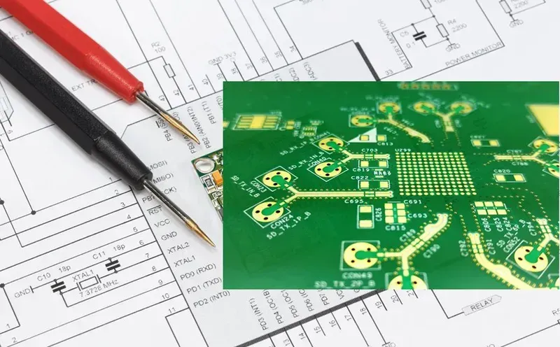
High-Frequency PCB Design
Designing Printed Circuit Boards (PCBs) for high-frequency power amplifiers, particularly those used in communication base stations, presents a unique array of technical hurdles. These challenges fundamentally stem from the demanding operational environment and the critical need for uncompromised signal integrity, efficient thermal management, and precise electrical performance, which are paramount for ensuring reliable and high-performance wireless communication networks.
Challenge Area
Description
Impact on Performance
Signal Integrity
Maintaining precise impedance control and minimizing signal loss and interference at high frequencies.
Leads to signal degradation, increased noise, and reduced amplifier efficiency, directly affecting communication quality and range.
Heat Dissipation High-power RF amplifiers generate significant heat, which must be efficiently dissipated to prevent component damage and maintain stable performance. Inadequate thermal management can lead to accelerated aging of components, performance degradation, and even catastrophic failure. This requires advanced thermal vias, heat sinks, and specific material selections that offer superior thermal conductivity, ensuring the longevity and reliability of the power amplifier.
Challenge Area
Description
Impact on Performance
Impedance Control
Achieving exact 50-ohm (or other specified) impedance matching across all RF transmission lines.
Mismatched impedance causes signal reflections (VSWR), power loss, and reduced amplifier output power and efficiency, impacting system stability.
Material Selection The choice of PCB substrate material is critical for high-frequency applications. Materials must possess low dielectric loss (Df), stable dielectric constant (Dk) across varying frequencies and temperatures, and excellent thermal stability. Standard FR-4 materials are often unsuitable due to higher losses and less predictable performance at RF frequencies, necessitating specialized laminates like Rogers, Arlon, or other ceramic-filled PTFE materials. The wrong material can severely compromise signal integrity and power efficiency.
Challenge Area
Description
Impact on Performance
Manufacturing Precision
Requiring extremely tight tolerances for trace widths, spacing, and layer registration.
Any deviation can lead to impedance variations, increased signal loss, and inconsistent performance across batches, affecting scalability and reliability.
Interference and EMI/EMC High-power RF circuits are susceptible to and can generate significant electromagnetic interference (EMI). Effective electromagnetic compatibility (EMC) design is crucial to prevent self-interference and interference with other sensitive components or systems. This involves careful grounding strategies, shielding techniques, filter integration, and optimal component placement to minimize radiated and conducted emissions, ensuring the amplifier operates cleanly within its designated spectrum.
Zero One Solution Limited's Expertise in High-Performance RF PCB Materials
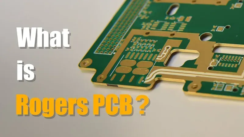
Rogers PCB Material
The performance of communication base station power amplifiers is fundamentally dependent on the underlying Printed Circuit Board (PCB) materials, which must withstand high frequencies, manage thermal loads, and maintain signal integrity. At Zero One Solution Limited, we leverage over a decade of specialized experience and strategic partnerships with leading material suppliers to provide superior RF PCB solutions. Our expertise lies in selecting and processing advanced dielectric materials that ensure optimal electrical performance, thermal management, and long-term reliability for the most demanding communication infrastructure applications, directly addressing the critical needs of next-generation base station technology.
Material Type
Key Properties for RF PAs
Typical Applications
Rogers Corporation (e.g., RO4000 Series)
Low dielectric loss (Df), excellent dimensional stability, high thermal conductivity, stable dielectric constant (Dk) across frequencies.
High-frequency RF circuits, base station antennas, power amplifiers, filters, and couplers.
Arlon Electronic Materials (e.g., CLTE Series)
Low Z-axis CTE (Coefficient of Thermal Expansion), superior thermal performance, high peel strength, excellent chemical resistance.
High-power RF/microwave applications, multi-layer PCBs for base stations, satellite communication systems.
Extremely low Dk and Df, high thermal stability, high moisture resistance, predictable performance.
MMIC packaging, radar systems, high-speed digital circuits, specialized base station modules.
Why are specialized RF PCB materials crucial for communication base station power amplifiers? Specialized RF PCB materials are crucial because standard FR-4 materials cannot meet the stringent demands of high-frequency and high-power applications found in base station power amplifiers. These amplifiers operate at frequencies where signal loss due to dielectric properties becomes significant. RF-specific materials, like those from Rogers or Arlon, offer stable dielectric constants (Dk) and extremely low dissipation factors (Df) across a wide range of frequencies and temperatures. This stability minimizes signal distortion, reduces power loss, and ensures consistent impedance control, which are all critical for efficient signal amplification and transmission in communication base stations. Without these materials, performance would degrade, leading to reduced coverage and network instability.
How does Zero One Solution Limited ensure thermal reliability with high-performance RF PCB materials? Zero One Solution Limited ensures thermal reliability through a multi-faceted approach. Firstly, we select materials with high thermal conductivity, such as certain Rogers laminates, which efficiently dissipate heat generated by the power amplifier components. Secondly, our design for manufacturability (DFM) analysis includes detailed thermal modeling and simulation to identify and mitigate potential hot spots. We also incorporate advanced thermal management features during PCB layout, such as specialized vias (thermal vias) and integrated heat sinks. Our manufacturing processes ensure precise lamination and material integration, creating robust thermal pathways that effectively transfer heat away from critical components, thereby prolonging the lifespan and maintaining the stable performance of the power amplifier in demanding base station environments.
Precision Manufacturing Processes for Communication Base Station Power Amplifier PCBs
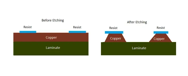
Precision PCB Etching
Achieving the highest performance in Communication Base Station Power Amplifier PCBs demands not only superior materials but also an unwavering commitment to precision in every manufacturing process. Zero One Solution Limited leverages advanced manufacturing techniques that are critical for maintaining signal integrity, managing thermal loads, and ensuring the long-term reliability required for the demanding telecom infrastructure. Our rigorous processes guarantee that even the most complex power amplifier PCB designs are realized with unmatched accuracy, directly contributing to the stable and efficient operation of base stations globally.
Precision Etching: The Foundation of RF Performance For high-frequency RF circuits, line width and spacing precision are paramount. Zero One Solution Limited employs state-of-the-art direct imaging (DI) and advanced etching technologies, including plasma etching for fine-line circuits, to achieve extremely tight tolerances. This precision minimizes impedance discontinuities and signal loss, which are critical for the demanding frequency ranges of communication base station power amplifiers, ensuring optimal signal propagation and power efficiency.
Multilayer Lamination: Building Robust RF Structures Power amplifier PCBs often incorporate complex multilayer structures to integrate various RF and control circuits while maintaining isolation and minimizing interference. We utilize advanced vacuum lamination techniques, precisely controlling temperature and pressure cycles, to ensure void-free and highly stable layer registration. This meticulous process is essential for achieving consistent dielectric thickness and impedance control across all layers, which is fundamental for high-frequency performance and thermal management in these critical components.
Surface Finishes: Optimizing Connectivity and Reliability The choice and application of surface finishes significantly impact the solderability, wire bonding capability, and long-term reliability of power amplifier PCBs. Zero One Solution Limited offers a range of high-performance surface finishes, including Electroless Nickel Immersion Gold (ENIG), Immersion Silver (ImAg), and Electroless Palladium Immersion Gold (ENEPIG). These finishes provide excellent flatness for fine-pitch components, superior signal transmission integrity for RF pads, and robust oxidation resistance, ensuring stable connections and extended operational life in harsh base station environments.
Automated Optical Inspection (AOI) and Electrical Testing: Assuring Quality To guarantee the flawless execution of intricate designs, every Communication Base Station Power Amplifier PCB undergoes stringent quality checks. We integrate advanced Automated Optical Inspection (AOI) systems that meticulously scan for defects, shorts, and opens, ensuring the integrity of the trace patterns. Furthermore, comprehensive electrical testing, including flying probe and fixture testing, validates circuit continuity, isolation, and adherence to specified impedance values, providing absolute assurance of functional performance before assembly.
Thermal Management Solutions Integration: Preventing Overheating Given the significant heat generation in power amplifiers, effective thermal management is integral to the PCB manufacturing process. Zero One Solution Limited incorporates specialized techniques such as integrating heavy copper layers, thermal vias, and metal core PCBs (MCPCBs) directly into the board design and manufacturing flow. Our processes ensure robust thermal pathways are created, efficiently dissipating heat away from critical components, thereby preventing performance degradation, extending component lifespan, and maintaining the reliability of the base station's power amplifier.
Comprehensive One-Stop Services: From Design to Assembly
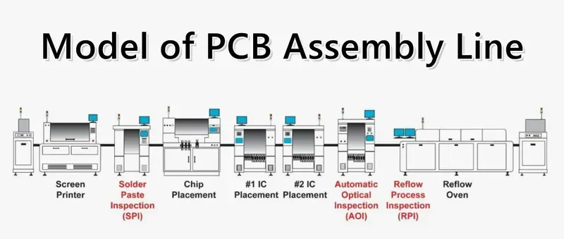
PCB Assembly Line
Zero One Solution Limited provides an unparalleled, integrated one-stop service for Communication Base Station Power Amplifier PCB Solutions, seamlessly guiding projects from initial conceptualization through to final assembly. This holistic approach significantly streamlines the development cycle, mitigating common challenges associated with fragmented supply chains and accelerating time-to-market for critical telecommunications infrastructure components. By consolidating design, manufacturing, and assembly under one roof, we empower our clients in the telecom industry to achieve exceptional efficiency and reliability.
Design for Manufacturability (DFM) and Design for Assembly (DFA) Analysis Our expert engineers meticulously review your power amplifier PCB designs for manufacturability and assembly efficiency. This proactive approach identifies potential issues early, optimizing the design for cost-effectiveness, yield, and performance before production begins. This minimizes costly revisions and ensures a smoother transition from design to mass production for communication base station power amplifier PCBs, critical for network stability and scalability.
Rapid Prototyping and Iteration Understanding the fast-paced nature of telecommunications R&D, we specialize in rapid prototyping of communication base station power amplifier PCBs. This allows for quick validation of designs, iterative improvements, and accelerated testing cycles, significantly reducing the overall development timeline. Our agility in producing high-quality prototypes ensures that innovative power amplifier designs can be quickly tested and refined for optimal performance in demanding base station environments.
Service Aspect
Benefit for Communication Base Station PA PCBs
Impact on Time-to-Market
DFM/DFA Analysis
Reduced design iterations, optimized production efficiency, enhanced reliability.
Up to 30% reduction in pre-production delays.
Rapid Prototyping
Quick validation of designs, accelerated testing, agile iteration.
Speeds up initial product validation by 40-50%.
Advanced Manufacturing
High-precision fabrication, consistent performance, adherence to stringent telecom standards.
High-accuracy component placement, reliable soldering, reduced human error.
Significantly reduces assembly time and post-assembly troubleshooting.
Integrated Supply Chain
Single point of contact, synchronized processes, comprehensive quality control.
Overall project timeline reduction by 20-25%.
How does Zero One Solution's one-stop service reduce costs for Communication Base Station Power Amplifier PCB projects? Our integrated one-stop service reduces costs by minimizing design iterations through DFM/DFA analysis, preventing costly manufacturing errors, and streamlining the supply chain. Consolidating services with a single vendor eliminates overheads from managing multiple suppliers, reduces shipping costs, and shortens project timelines, directly translating into significant cost savings for high-performance communication base station power amplifier PCBs.
What specific quality control measures are in place for Communication Base Station Power Amplifier PCB assembly? For communication base station power amplifier PCB assembly, we implement a multi-stage quality control process. This includes automated optical inspection (AOI) for solder joint integrity and component placement, X-ray inspection for hidden connections like BGAs, in-circuit testing (ICT) for electrical functionality, and final functional testing (FCT) tailored to the specific power amplifier's performance requirements. All processes adhere to IPC standards to ensure the highest reliability crucial for base station operation.
How does Zero One Solution handle urgent or high-volume orders for Communication Base Station Power Amplifier PCBs? Leveraging our strategic location in Shenzhen, China's electronic manufacturing hub, and our robust global PCBA supply chain network, Zero One Solution is uniquely positioned to handle both urgent rapid prototyping and high-volume production for communication base station power amplifier PCBs. Our flexible manufacturing lines, optimized processes, and established material sourcing channels enable us to scale production efficiently while maintaining stringent quality standards, ensuring timely delivery for demanding telecom projects.
The demands placed on communication base station power amplifiers will only intensify with the advent of 5G, 6G, and beyond. Zero One Solution Limited is not just a PCB manufacturer; we are a strategic partner dedicated to empowering innovation. Our deep expertise, rapid prototyping capabilities, and comprehensive one-stop services from design to assembly ensure that your power amplifier PCBs meet the highest standards of performance, reliability, and efficiency. Headquartered in Shenzhen and with a branch in Dubai, our global supply chain network ensures seamless support for your projects, anywhere in the world. Choose Zero One Solution Limited for your next communication base station power amplifier PCB project and experience the difference that experience, expertise, and a commitment to excellence can make. Contact us today to discuss how we can help accelerate your product development and bring your next-generation telecom solutions to life.