In today's visually driven world, the clarity, speed, and intelligence of digital cameras are paramount. From professional photography to advanced industrial inspection and medical imaging, the performance of a digital camera hinges critically on its internal image processing board. At Zero One Solution Limited, we understand that bringing innovative vision products to market demands not just robust hardware, but also lightning-fast development cycles and unparalleled technical expertise. As a leading PCB solution provider specializing in rapid prototyping, we're here to delve into how our Digital Camera Image Processing Board Solution empowers companies like yours to achieve groundbreaking imaging capabilities with exceptional efficiency and precision.
The Core of Digital Imaging: Image Processing Boards
Digital Camera Image Processing Board
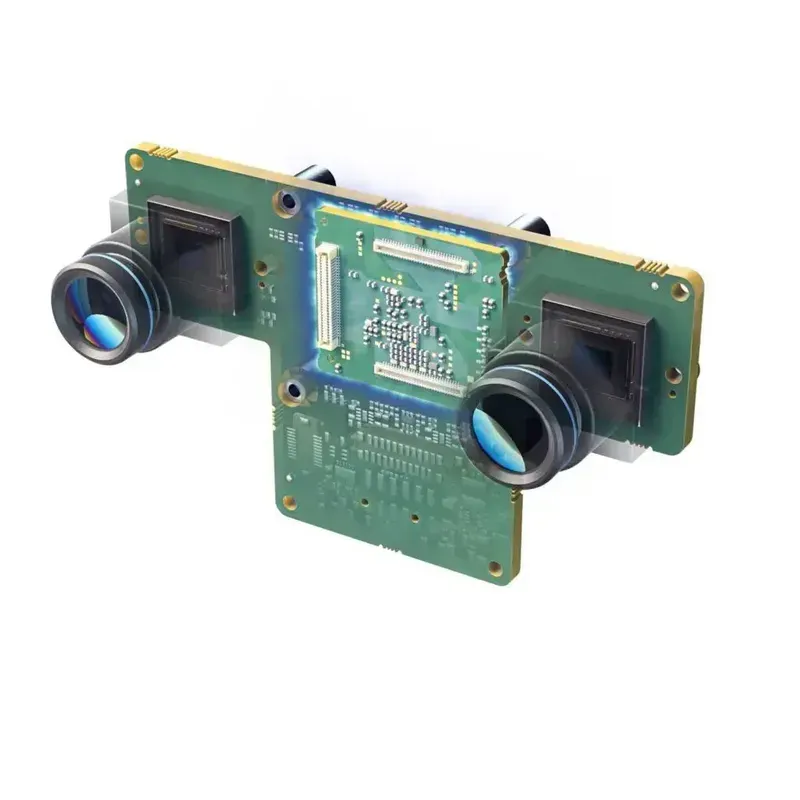
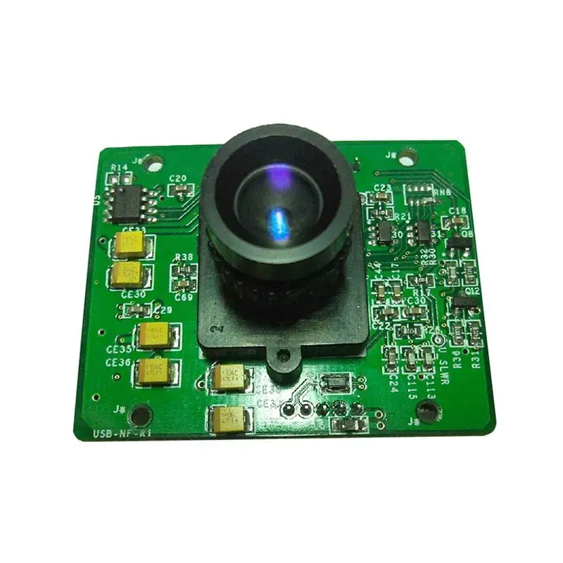
The digital camera image processing board is the foundational component that transforms raw sensor data into the stunning images we see, acting as the brain behind the lens. It orchestrates the entire imaging pipeline, from initial signal acquisition and noise reduction to color correction, compression, and final image rendering. Zero One Solution Limited, with its deep expertise in high-performance PCB solutions, understands that the board's design directly impacts image quality, processing speed, and overall camera performance, making it a critical differentiator in the competitive digital imaging market.
What is the primary function of an image processing board in a digital camera? The primary function of an image processing board is to convert raw electrical signals captured by the camera's image sensor into a usable digital image format. This involves a complex series of computations including analog-to-digital conversion, noise reduction, white balance, color correction, demosaicing, sharpening, compression, and formatting for storage or display.
Why is the image processing board considered the "brain" of a digital camera? The image processing board is considered the "brain" because it houses the crucial integrated circuits, such as Digital Signal Processors (DSPs) and Field-Programmable Gate Arrays (FPGAs), that execute the sophisticated algorithms required for real-time image manipulation. It controls the flow of data, manages memory, and handles the intricate calculations that transform light into a coherent visual representation, much like a brain processes sensory input.
How does Zero One Solution ensure high performance in image processing board designs? Zero One Solution ensures high performance by meticulously designing PCBs that accommodate high-speed data interfaces (e.g., MIPI, LVDS), optimize signal integrity, manage thermal dissipation, and integrate powerful processing units. Our rapid prototyping and advanced manufacturing capabilities enable us to validate designs quickly, ensuring superior processing power and efficient data handling critical for high-resolution and high-frame-rate imaging.
What are the key components found on a typical digital camera image processing board? Key components typically found on an image processing board include the Image Signal Processor (ISP), which performs core image pipeline functions; a main System-on-Chip (SoC) or Microcontroller Unit (MCU); high-speed memory (e.g., LPDDR4/5) for buffering and processing; power management ICs; and various interfaces for sensor input, display output, storage (SD card controller), and connectivity (USB, Wi-Fi).
Key Challenges in Digital Camera PCB Design
Digital Camera PCB Design
Designing the Printed Circuit Board (PCB) for a digital camera's image processing unit presents a unique set of engineering challenges that are critical to achieving superior image quality and product reliability. These challenges span from managing high-speed data flows to optimizing power consumption and ensuring thermal stability within a compact form factor. Overcoming these hurdles is paramount for any digital camera manufacturer aiming to deliver high-performance, competitive products. Zero One Solution Limited, with its deep expertise in rapid prototyping and advanced PCB design, specializes in navigating these complexities to deliver robust and efficient image processing board solutions.
High-Speed Data Transfer and Signal Integrity Digital cameras generate immense volumes of raw image data at incredibly high speeds. Designing PCBs to reliably transmit this data without signal degradation (e.g., crosstalk, reflections) requires meticulous impedance matching, controlled trace routing, and advanced differential pair techniques. Challenges include maintaining signal integrity at gigabit speeds for interfaces like MIPI DSI/CSI and LVDS, which are crucial for clear image transmission from sensor to processor. Zero One Solution employs advanced simulation tools and adheres to IPC standards to ensure optimal signal integrity, even under extreme conditions, critical for flawless image data flow.
Power Efficiency and Thermal Management Modern digital cameras demand high computational power for real-time image processing, often in small, portable devices. This creates a dual challenge: maximizing power efficiency to extend battery life and effectively dissipating heat generated by high-performance components like DSPs and FPGAs. Inadequate thermal management can lead to performance throttling, component failure, and reduced product lifespan. Our design approach integrates power-efficient component selection, optimized power delivery networks (PDN), and sophisticated thermal analysis (e.g., heat sinks, thermal vias) to ensure stable operation and longevity, even in demanding photographic scenarios.
Miniaturization and Component Density The drive for thinner, lighter, and more compact digital cameras necessitates extremely dense PCB layouts. This involves placing numerous components, including image sensors, processors, memory, and power management units, in a confined space while maintaining electrical performance and manufacturability. This challenge requires multi-layer PCBs, fine-pitch component placement, and advanced routing strategies. Zero One Solution leverages high-density interconnect (HDI) technology and expertise in micro-via and blind/buried via fabrication to achieve highly compact and functional image processing boards, enabling sleek product designs.
Zero One Solution's Comprehensive Image Processing Board Solution
PCB Manufacturing and Assembly Line
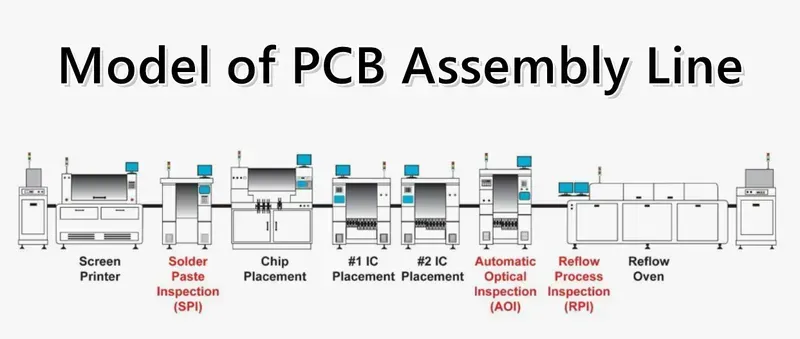
Zero One Solution Limited provides a holistic, end-to-end service for digital camera image processing board solutions, encompassing every critical stage from initial concept to final assembly. This integrated approach not only streamlines the development process but also ensures superior performance and reliability, establishing us as a leading partner for innovation in digital imaging. Our comprehensive solution is designed to navigate the complexities of high-speed data, intricate circuit designs, and stringent quality demands inherent in advanced camera systems.
Service Stage
Description
Zero One Solution's Advantage
Concept & Schematic Design
Translating initial product ideas into detailed electronic schematics, defining component selection and interconnectivity.
Expert engineers with deep understanding of image signal processing (ISP) pipelines and sensor interfaces, ensuring optimal architectural foundation for digital camera image processing board solutions, aligning with client's specific performance requirements and cost targets, avoiding costly redesigns later.
Service Stage
Description
Zero One Solution's Advantage
PCB Layout & Design
Transforming schematics into physical PCB layouts, considering signal integrity, power distribution, thermal management, and compact form factors.
Utilization of advanced EDA tools and DFM (Design for Manufacturability) principles to optimize impedance matching, minimize EMI/EMC, and ensure efficient routing for high-speed signals like MIPI and LVDS, crucial for digital camera image processing boards.
Service Stage
Description
Zero One Solution's Advantage
Rapid Prototyping
Quick turnaround manufacturing of initial PCB samples for testing and validation.
Industry-leading rapid prototyping capabilities, significantly reducing time-to-market and allowing for agile design iterations, which is critical for digital camera product development cycles.
Service Stage
Description
Zero One Solution's Advantage
Manufacturing & Assembly
High-volume production of PCBs and assembly of all components onto the board, including rigorous quality control.
State-of-the-art manufacturing facilities in Shenzhen and a global supply chain network, ensuring cost-effective, high-quality production with stringent adherence to IPC standards, guaranteeing robust digital camera image processing board solutions.
Why choose Zero One Solution for your digital camera image processing board needs? We offer a distinct competitive advantage through our one-stop, integrated service model. Unlike engaging multiple vendors, our comprehensive approach ensures seamless communication, reduced lead times, and unified quality control from design conceptualization through to final assembly. This minimizes project complexity, mitigates risks, and ultimately accelerates your product's journey to market, providing a singular point of accountability and expertise for your digital camera image processing board solution.
Advanced Technologies for Superior Image Quality
DSP and FPGA Chips
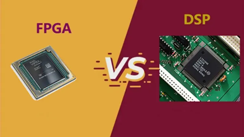
Achieving superior image quality in digital cameras hinges on the integration of cutting-edge technologies within the image processing board. Zero One Solution Limited leverages its deep expertise to incorporate high-performance digital signal processors (DSPs), field-programmable gate arrays (FPGAs), and specialized high-speed interfaces, forming the bedrock for exceptional visual fidelity and processing efficiency, which are critical for delivering a premium user experience and maintaining a competitive edge in the market.
High-Performance DSPs and FPGAs Our solutions integrate state-of-the-art DSPs and FPGAs, which are indispensable for handling the intensive computational demands of image processing. DSPs excel in real-time filtering, noise reduction, and color correction, while FPGAs provide unparalleled flexibility and parallel processing capabilities, ideal for custom image pipelines and rapid algorithmic updates. This synergy ensures precise image manipulation and a foundation for advanced features like computational photography. For instance, high-end digital cameras often utilize multi-core DSPs capable of processing hundreds of megapixels per second, supported by FPGAs that can be reconfigured to optimize specific image processing algorithms post-manufacturing, a significant advantage for product evolution and responsiveness to market demands. According to a report by MarketsandMarkets, the global image processing market is projected to grow significantly, driven by advancements in these core components, highlighting their strategic importance in product differentiation and performance leadership.
Technology
Key Benefit
Application in Digital Camera Image Processing
High-Performance DSPs
Real-time image enhancement, noise reduction, color correction
Rapid processing of RAW sensor data, accurate color reproduction, advanced computational photography features like HDR and panoramic stitching
FPGAs
Flexibility, parallel processing, customizability
Accelerated image pipeline execution, on-the-fly algorithm adaptation, low-latency video streaming, custom hardware acceleration for AI-based image processing
High-Speed Interfaces (MIPI, LVDS)
Efficient data transfer, low power consumption
Seamless communication between image sensor and ISP, supporting high-resolution and high-frame-rate video capture
Specialized Memory Solutions
Fast data access, high bandwidth
Efficient buffering of large image frames, support for burst shooting and high-resolution video recording (e.g., LPDDR5, GDDR6 for high-end systems)
Optimized High-Speed Interfaces To ensure uncompromised data integrity and speed, Zero One Solution meticulously designs boards with optimized high-speed interfaces such as MIPI (Mobile Industry Processor Interface) and LVDS (Low-Voltage Differential Signaling). These interfaces are crucial for efficiently transferring vast amounts of raw image data from the sensor to the processing unit without bottlenecks, enabling high-resolution capture and rapid burst modes. Our design considerations include impedance matching, signal integrity, and crosstalk mitigation to ensure robust and reliable data transmission, which is paramount for maintaining image fidelity from capture to output. A poorly designed interface can introduce noise or data loss, directly impacting the final image quality and the camera's overall performance. This attention to detail in interface design ensures that the high-resolution data captured by advanced sensors is fully utilized by the processing pipeline, translating directly into sharper, clearer images.
Rapid Prototyping: Accelerating Your Product Development
PCB Rapid Prototyping
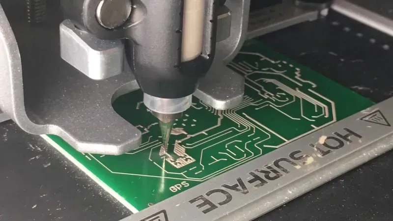
In the fast-evolving digital camera market, speed to market is paramount. Zero One Solution's rapid prototyping capabilities are specifically designed to empower innovators, significantly reducing the development cycle for your digital camera image processing board solutions. Our agile approach ensures that your cutting-edge designs transition from concept to tangible, testable prototypes with unparalleled efficiency, giving you a critical competitive advantage.
Streamlined Design-to-Prototype Workflow Zero One Solution integrates advanced CAD/CAM systems with automated manufacturing processes to facilitate a seamless transition from your digital camera PCB design files to physical prototypes. This minimizes manual intervention and potential errors, ensuring precision and fidelity to your original specifications. Our workflow is optimized for iterative design, allowing for quick modifications and re-prototyping.
Expedited Component Sourcing and Assembly Leveraging our extensive global supply chain network and strategic presence in Shenzhen and Dubai, we secure high-quality, specialized components for digital camera image processing boards rapidly. Our advanced SMT and assembly lines are equipped to handle complex, high-density layouts, ensuring quick turnaround times for even the most intricate digital camera PCB prototypes. This includes specialized DSPs, FPGAs, and high-speed connectors critical for image processing.
Aspect
Traditional Prototyping
Zero One Solution Rapid Prototyping
Lead Time
Weeks to Months
Days to Weeks
Iteration Speed
Slow, Costly
Fast, Cost-Effective
Risk Profile
High Rework Risk
Reduced Design Flaws
Cost Efficiency
Higher Initial Investment
Optimized, Lower Overall Cost
Market Entry
Delayed
Accelerated
By significantly compressing development timelines and facilitating rapid design iterations, Zero One Solution empowers digital camera manufacturers to innovate faster, validate designs more efficiently, and bring their next-generation imaging products to market ahead of the competition. Our rapid prototyping is not just about speed; it's about intelligent, agile development that ensures your digital camera image processing board is perfected quickly and reliably.
Quality Assurance and Reliability in Digital Camera Electronics
PCB Testing and Quality Control
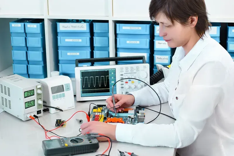
In the demanding realm of digital camera electronics, where capturing fleeting moments with pristine clarity is paramount, the reliability and long-term performance of image processing boards are non-negotiable. Zero One Solution Limited implements a multi-layered, rigorous quality assurance framework to guarantee the robustness and longevity of every digital camera image processing board, ensuring they consistently perform flawlessly under diverse operational conditions. Our commitment extends beyond mere functionality, focusing on stability, thermal resilience, and signal integrity to deliver unparalleled dependability in your imaging solutions.
How does Zero One Solution ensure signal integrity for high-speed digital camera image processing? We employ advanced signal integrity (SI) and power integrity (PI) analysis during the design phase, utilizing sophisticated simulation tools to predict and mitigate issues like crosstalk, reflections, and ground bounce. This is complemented by careful material selection for PCBs, controlled impedance routing, and optimized stack-up designs, ensuring pristine signal transmission for high-resolution image data at high frequencies. Post-manufacturing, TDR (Time Domain Reflectometry) testing verifies impedance matching and trace characteristics, guaranteeing signal fidelity.
What thermal management strategies are integrated into digital camera image processing board solutions? Effective thermal management is crucial for high-performance image processing units. Zero One Solution designs incorporate advanced thermal dissipation techniques, including optimized component placement for airflow, strategic use of thermal vias, and consideration of heat sinks or thermal pads where necessary. We conduct comprehensive thermal simulations (CFD analysis) early in the design cycle and validate with thermal imaging during prototyping and testing to ensure optimal operating temperatures and prevent performance degradation or component failure due to heat.
What environmental testing protocols are applied to digital camera image processing boards? Our quality assurance extends to comprehensive environmental testing to validate board resilience. This includes accelerated life testing (ALT), thermal cycling, humidity testing, and vibration/shock testing to simulate real-world operating conditions and stress factors. These rigorous tests ensure the digital camera image processing boards maintain performance and structural integrity across various climates and physical demands, guaranteeing long-term reliability in the field.
QA Metric
Description
Zero One Solution Approach
IPC Standards Compliance
Adherence to industry-recognized standards for PCB manufacturing and assembly.
Strict compliance with IPC-A-610 (Acceptability of Electronic Assemblies) and IPC-6012 (Qualification and Performance Specification for Rigid Printed Boards), ensuring high-quality fabrication and assembly processes.
In conclusion, the demands on digital camera image processing boards are ever-increasing, requiring a blend of high performance, efficiency, and rapid innovation. Zero One Solution Limited stands as your premier partner, offering a comprehensive Digital Camera Image Processing Board Solution that encompasses everything from expert PCB design and rapid prototyping to full-scale manufacturing and assembly. Our commitment to quality, speed, and customer-centric service, backed by our strategic global presence, ensures that your vision projects transition from concept to market with unmatched acceleration. Don't let complex electronics be a barrier to your imaging breakthroughs. Partner with Zero One Solution and transform your digital camera ambitions into reality. Contact us today to discuss how our bespoke solutions can elevate your next-generation imaging product.