In an era where sustainable energy and efficient resource utilization are paramount, distributed energy management has emerged as a cornerstone of modern power systems. From smart grids to renewable energy integration, the ability to precisely control and distribute energy is critical. This complex challenge often boils down to the foundational hardware: the Printed Circuit Board (PCB). Zero One Solution Limited, a leader in rapid prototyping and one-stop PCB solutions, understands this intrinsic link. This article delves into how our specialized PCB solutions are empowering the next generation of distributed energy management systems, accelerating innovation and ensuring reliable power delivery.
The Imperative for Distributed Energy Management
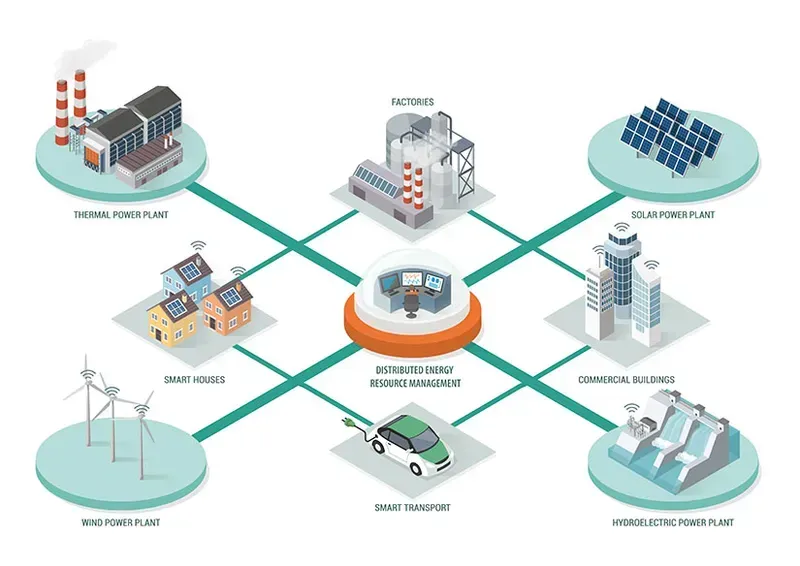
The global energy landscape is undergoing a profound transformation, shifting from centralized power generation to a decentralized model driven by an urgent need for sustainability, efficiency, and grid resilience. This paradigm shift, known as Distributed Energy Management (DEM), integrates diverse energy sources like solar, wind, and battery storage directly into local grids, revolutionizing how power is generated, consumed, and managed. This distributed approach addresses critical challenges such as reducing carbon emissions, enhancing energy independence, and fortifying grid stability against disruptions. By enabling real-time monitoring and control of energy flows, DEM systems are not just an evolution but a fundamental necessity for a cleaner, more reliable, and decentralized energy future.
Driving Factor
Description
Impact on Energy Management
Renewable Energy Integration
Incorporation of intermittent sources like solar PV and wind turbines.
Requires sophisticated control to balance supply and demand, manage intermittency, and ensure grid stability.
Grid Stability & Resilience
Vulnerability of centralized grids to outages and cyber threats.
DEM decentralizes risk, enabling localized power supply during outages and enhancing overall grid robustness.
Energy Efficiency & Cost Reduction
Minimizing transmission losses and optimizing energy consumption.
Allows for localized energy generation closer to consumption points, reducing losses and enabling demand-side management.
Challenges in Centralized Energy Systems Traditional centralized energy grids face inherent inefficiencies due to long-distance transmission losses, susceptibility to single points of failure, and limited flexibility in integrating diverse renewable energy sources. This model often results in higher operational costs and a less resilient energy infrastructure, particularly in the face of increasing energy demand and climate volatility.
Benefits of Distributed Energy Systems Distributed energy systems offer significant advantages, including reduced transmission losses by generating power closer to the point of consumption, enhanced grid resilience through decentralized energy assets, and greater flexibility for integrating intermittent renewable energy sources. They empower communities and businesses with greater energy independence and control over their consumption profiles, fostering a more sustainable and robust energy ecosystem.
Role of PCBs in Energy Management Systems
PCB in Distributed Energy Management System
Printed Circuit Boards (PCBs) serve as the foundational backbone for all electronic control units within modern Distributed Energy Management (DEM) systems. Their critical function extends beyond mere circuit interconnection; PCBs are the unsung heroes enabling the sophisticated communication, efficient power conversion, and robust data processing that are indispensable for the seamless operation and optimization of decentralized energy grids. Without advanced PCB technology, the promise of renewable energy integration and smart grid functionality would remain largely unfulfilled.
Communication Hubs PCBs facilitate the intricate network of data exchange within DEM systems. They host microcontrollers, transceivers, and communication interfaces (e.g., Ethernet, Wi-Fi, RS-485, CAN bus) that allow various components—solar inverters, battery management systems, smart meters, and grid controllers—to communicate real-time energy data. This real-time information exchange is vital for dynamic load balancing, fault detection, and predictive maintenance.
Power Conversion and Distribution In distributed energy, power frequently needs conversion between AC and DC, and voltage levels adjusted. PCBs are integral to power electronics, supporting high-current traces, heat dissipation structures, and robust component mounting for inverters, converters, and charge controllers. They ensure efficient and safe power flow from diverse sources to consumption points or storage units.
Data Acquisition and Processing DEM systems rely heavily on sensors to monitor parameters like voltage, current, temperature, and power consumption. PCBs are the platform for these sensor interfaces and the initial stage of data processing. They integrate Analog-to-Digital Converters (ADCs) and Digital Signal Processors (DSPs) that collect raw data, convert it into usable information, and transmit it for higher-level analysis and decision-making by energy management algorithms.
Control and Automation The intelligence of DEM systems, from automated switching to grid synchronization, resides on PCBs. They house the embedded processors and control logic that execute complex algorithms for energy optimization, demand-side management, and grid stabilization. This enables autonomous responses to grid fluctuations and optimizes energy dispatch based on real-time conditions and predefined strategies.
PCB Function in DEM
Key Components Involved
Impact on System Performance
Signal Integrity
Traces, vias, ground planes, impedance control
Ensures accurate data transmission, prevents noise interference, critical for precise control.
Thermal Management
Copper pours, thermal vias, heatsinks, material selection
Dissipates heat from power components, extends component lifespan, maintains operational stability.
Reduces electromagnetic interference, ensures compliance with industry standards, improves system reliability.
Reliability & Durability
High Tg laminates, robust soldermask, conformal coating
Withstands harsh environmental conditions, ensures long-term operation in outdoor or industrial settings.
Key PCB Design Considerations for Distributed Energy Management Solutions
Energy PCB Design Considerations
Designing Printed Circuit Boards (PCBs) for distributed energy management (DEM) systems requires a meticulous approach, as these boards are the linchpin for efficient power conversion, communication, and control in highly demanding environments. Unlike general-purpose electronics, DEM PCBs face unique challenges such as managing high current densities, dissipating significant heat, ensuring robust signal integrity amidst electrical noise, and guaranteeing long-term reliability under varying operational conditions. Addressing these considerations during the design phase is paramount to developing stable, efficient, and resilient distributed energy infrastructure. Engineers must prioritize robust design principles to create PCBs capable of withstanding the rigors of continuous energy flow and dynamic load changes.
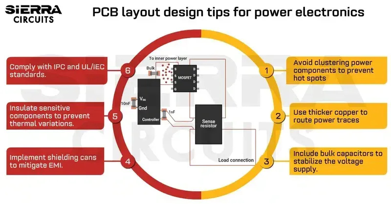
High Current Handling and Power Density Distributed energy systems often involve significant power levels, necessitating PCBs capable of safely and efficiently handling high currents. This demands wider copper traces, thicker copper weights (e.g., 2oz, 3oz, or even heavier copper for power planes), and appropriate trace spacing to prevent overheating and voltage drops. Multi-layer designs with dedicated power and ground planes are critical for distributing current uniformly and minimizing impedance. Simulation tools for current density and thermal analysis are essential to validate these designs before fabrication, ensuring the PCB can sustain peak operational loads without compromise.
Delamination, performance degradation at high temperatures
Advanced Thermal Management Heat generation is an inherent challenge in power electronics, and DEM PCBs are no exception. Effective thermal management is crucial for maintaining component longevity and system performance. Design strategies include incorporating large copper pours for heat spreading, using thermal vias to transfer heat to other layers or heatsinks, and optimizing component placement to avoid hot spots. For high-power components like MOSFETs and IGBTs, direct attachment to metal core PCBs (MCPCBs) or the use of external heatsinks with thermal interface materials becomes critical. Computational Fluid Dynamics (CFD) simulations are often employed to predict thermal behavior and optimize cooling solutions.
Ensuring optimal signal integrity and electromagnetic compatibility (EMC) is another pivotal design consideration. DEM environments are often noisy, with switching power supplies and high-frequency transients. Proper grounding techniques, controlled impedance traces, differential signaling, and strategic component placement are vital to minimize electromagnetic interference (EMI) and ensure reliable data communication between various control units. The longevity and reliability of PCBs in DEM applications are paramount, given the often remote or critical nature of these systems. This necessitates the use of robust materials, comprehensive design-for-reliability (DFR) analyses, and rigorous environmental testing to ensure the boards can withstand temperature extremes, humidity, vibration, and mechanical stress over their operational lifespan.
Zero One Solution's Expertise in Distributed Energy Management PCBs
PCB Rapid Prototyping
Zero One Solution Limited stands at the forefront of providing specialized PCB solutions for Distributed Energy Management (DEM) systems, leveraging over a decade of experience and a strategic presence in global manufacturing hubs. Our expertise is not merely in fabricating boards, but in understanding the intricate demands of power electronics, signal integrity, and long-term reliability essential for decentralized energy infrastructure. We empower our clients to accelerate innovation and deployment of critical energy solutions through our rapid prototyping capabilities, sophisticated manufacturing processes, and unparalleled ability to handle complex control board designs, all underpinned by a seamless one-stop service.
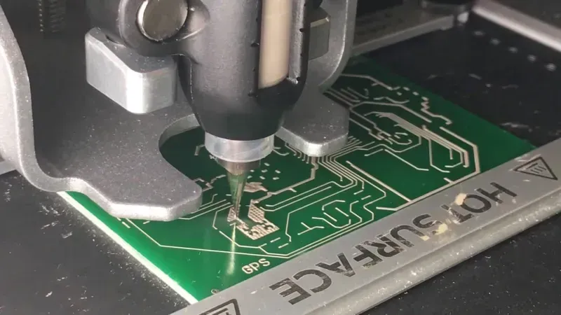
Rapid Prototyping for Accelerated Development We understand the critical need for speed in the rapidly evolving energy sector. Our rapid prototyping services significantly reduce lead times, enabling quick design iterations and validation, which is crucial for bringing cutting-edge DEM solutions to market faster. This agility allows engineers to test and refine their concepts efficiently, minimizing risks and development costs.
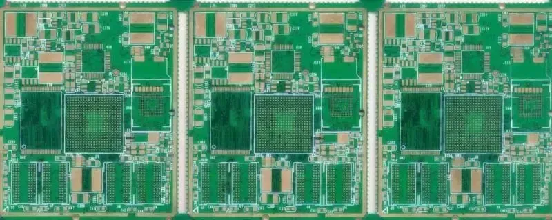
Advanced Manufacturing Processes for High Performance Our manufacturing facilities are equipped with state-of-the-art technology to produce PCBs that meet the rigorous demands of distributed energy applications. This includes precision fabrication for multi-layer boards, fine-line technology for high-density interconnects, and robust surface finishes to ensure optimal performance and longevity in diverse operational environments. We adhere strictly to industry standards such as IPC Class 2/3.
Capability
Description
Benefit to DEM Solutions
Complex Power Electronics Handling
Expertise in designing and manufacturing PCBs for high-current, high-voltage power conversion modules, essential for solar inverters, battery management systems, and grid-tied devices.
Ensures efficient power conversion, reduced energy loss, and robust operation under demanding electrical loads, enhancing system reliability and performance.
:Intricate Control Board Designs
Proficiency in integrating sensitive analog and digital circuits on PCBs for precise monitoring, control, and communication within DEM networks.
Facilitates accurate data acquisition, intelligent decision-making, and seamless communication between distributed energy assets, crucial for optimized energy flow and grid stability.
Seamless One-Stop Service from Design to Assembly From initial concept and PCB design consultation to precise manufacturing and final assembly, Zero One Solution Limited offers an integrated, end-to-end service. This holistic approach streamlines the entire product development lifecycle, reducing coordination complexities and ensuring consistent quality across all stages, making us a reliable partner for your DEM projects.
Advanced Materials and Manufacturing for Reliability
High-Tg Laminate PCB Material
The long-term reliability and peak performance of Printed Circuit Boards (PCBs) in distributed energy management systems are fundamentally dependent on the judicious selection of advanced materials and the application of precise manufacturing techniques. These systems often operate in challenging environments, enduring significant temperature fluctuations, high current loads, and mechanical stresses. Therefore, the choice of substrate, copper thickness, and surface finishes directly dictates a PCB's ability to withstand these conditions and maintain operational integrity over its extended lifespan, ultimately ensuring the stability and efficiency of the energy grid.
High-Performance Laminates For demanding distributed energy applications, standard FR-4 may not suffice. High-Tg (Glass Transition Temperature) laminates are crucial as they maintain their mechanical and electrical properties at elevated temperatures, preventing delamination and ensuring signal integrity under thermal stress. Low Dk/Df materials are also important for high-frequency power conversion stages to minimize signal loss and improve efficiency.
Heavy Copper PCB Technology Distributed energy systems, particularly those involving power conversion or high-current transmission, necessitate heavy copper PCBs. Unlike standard PCBs (typically 1 oz copper), heavy copper boards (3 oz to 20 oz or more) reduce thermal resistance, enhance current carrying capacity, and improve mechanical strength, significantly mitigating hot spots and increasing overall system reliability.
Advanced Surface Finishes The surface finish protects the exposed copper circuitry and ensures solderability. Immersion Gold (ENIG) offers excellent planarity for fine-pitch components and good shelf life, while Hard Gold is suitable for high-wear areas like edge connectors. Lead-free HASL is a cost-effective option for less demanding applications, but its thermal properties must be considered for high-power designs.
Rigid-Flex PCB Solutions For compact and complex distributed energy modules, rigid-flex PCBs offer a robust solution by integrating rigid sections with flexible interconnections. This eliminates the need for connectors, reduces assembly time, improves signal integrity, and provides superior shock and vibration resistance, critical for outdoor or mobile energy applications.
Material/Technique
Key Benefit for Distributed Energy
Typical Application
High-Tg Laminates
Enhanced thermal stability, prevents delamination
Inverters, battery management systems
Heavy Copper
High current capacity, improved thermal management
Power converters, bus bars, solar array combiners
ENIG Surface Finish
Excellent solderability, long shelf life, fine pitch
From Design to Assembly: Our Comprehensive Solution
PCB Design to Assembly Process
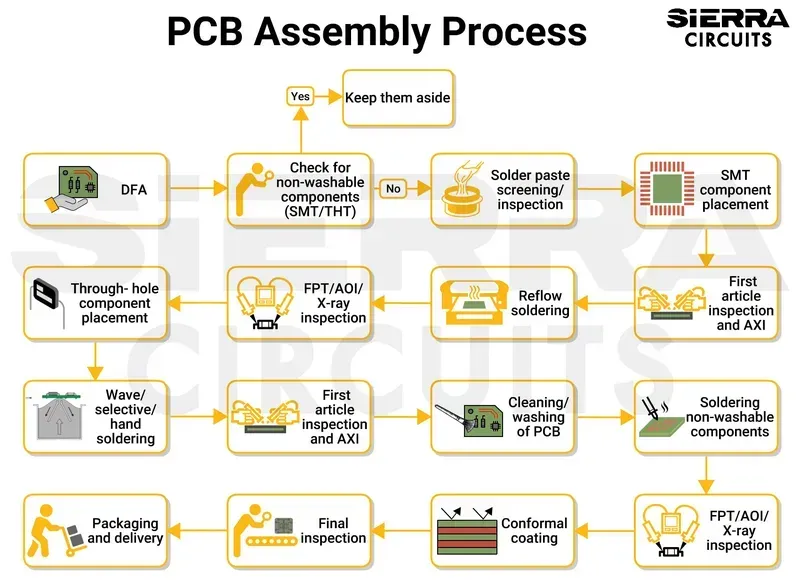
Zero One Solution Limited provides a streamlined, comprehensive "Design to Assembly" service for Distributed Energy Management (DEM) PCBs, eliminating the complexities of managing multiple vendors. This integrated approach ensures seamless project execution, from initial concept to final product, significantly accelerating time-to-market for critical energy solutions. Our end-to-end capabilities are particularly vital in the DEM sector, where precision, reliability, and rapid deployment are paramount.
Integrated Service Benefits for DEM PCBs Our unified approach integrates all stages of PCB development, from design and prototyping to manufacturing and assembly. This reduces potential communication gaps, minimizes errors, and ensures consistent quality control throughout the entire production cycle, critical for complex DEM systems.
Service Stage
Key Activities
Benefits for DEM Solutions
PCB Design Consultation
Schematic capture, layout optimization, DFM/DFA analysis for high-power applications.
Ensures optimal electrical performance, thermal dissipation, and manufacturability from the outset, crucial for robust DEM systems.
Service Stage
Key Activities
Benefits for DEM Solutions
Rapid Prototyping
Quick-turnaround fabrication of functional prototypes for testing and validation.
Accelerates R&D cycles, enabling rapid iteration and validation of designs for distributed energy infrastructure.
Service Stage
Key Activities
Benefits for DEM Solutions
Advanced Manufacturing
Utilizing high-Tg laminates, heavy copper, and precision fabrication for demanding energy environments.
Guarantees PCBs can withstand the harsh operational conditions and high current loads typical in distributed energy applications.
Delivers fully functional, tested PCB assemblies, ready for integration into larger DEM systems, reducing client's post-production effort.
By offering a single point of contact and accountability, Zero One Solution Limited simplifies the procurement and development process, allowing our clients in the energy sector to focus on their core innovation, secure in the knowledge that their PCB solutions are handled by a trusted, experienced partner. This comprehensive service model is specifically tailored to meet the demanding requirements and accelerated timelines of the distributed energy market.
Future Trends and Our Vision in Distributed Energy
The landscape of distributed energy management (DEM) is rapidly evolving, driven by technological innovations that promise greater efficiency, resilience, and sustainability. As renewable energy penetration increases and grid modernization accelerates, the demand for sophisticated PCB solutions that can support these advancements becomes paramount. Zero One Solution Limited is strategically positioned to not only meet these current demands but also to anticipate and shape the future of DEM through cutting-edge PCB technology and relentless innovation.
AI-Powered Energy Management Artificial Intelligence (AI) is revolutionizing DEM by enabling predictive analytics for energy generation and consumption, optimizing energy flow, and facilitating proactive maintenance. PCBs for these systems require high-density integration, robust signal integrity, and efficient power delivery to support powerful AI processors and complex algorithms. Our advanced design and manufacturing capabilities ensure that the control boards can handle the computational demands of AI-driven energy optimization.
IoT Integration and Edge Computing The Internet of Things (IoT) is expanding the reach of DEM, connecting countless sensors and devices across the energy grid. This proliferation necessitates edge computing capabilities to process data closer to the source, reducing latency and improving responsiveness. PCBs designed for IoT and edge applications must be compact, low-power, and highly reliable, often operating in diverse environmental conditions. Zero One Solution excels in producing miniaturized, high-performance PCBs critical for these distributed intelligent nodes.
Enhanced Cybersecurity for Grid Resilience As DEM systems become more interconnected, cybersecurity becomes a critical concern. Protecting against cyber threats requires secure hardware foundations, including specialized PCBs that integrate secure elements, encryption modules, and tamper-detection features. Our commitment to high-reliability manufacturing and component sourcing ensures the physical security of the electronic backbone, contributing to the overall resilience and trustworthiness of distributed energy infrastructure.
Advanced Energy Storage Solutions The integration of advanced battery energy storage systems (BESS) is crucial for stabilizing grids with high renewable penetration. PCBs in BESS are subjected to high currents, thermal cycling, and demands for precise battery management. Our expertise in heavy copper PCBs, effective thermal management, and robust interconnection technologies enables the development of highly efficient and safe battery management systems (BMS) for these critical applications.
Vehicle-to-Grid (V2G) Technology V2G technology, allowing electric vehicles to both draw from and feed energy back into the grid, represents a significant future trend. This bidirectional power flow necessitates sophisticated power electronics and control PCBs capable of managing high power transfer, ensuring grid synchronization, and protecting against electrical transients. Our experience with high-power, high-frequency PCB designs positions us as an ideal partner for V2G innovators.
Zero One Solution Limited's vision is to be at the forefront of enabling the next generation of distributed energy management. By continuously investing in advanced manufacturing processes, exploring novel materials, and collaborating closely with our clients, we aim to provide the foundational PCB technology that powers a more sustainable, resilient, and intelligent energy future. Our rapid prototyping and comprehensive one-stop services ensure that our partners can innovate and deploy their solutions faster and more reliably than ever before.
Frequently Asked Questions about Distributed Energy Management PCBs
Navigating the complexities of Distributed Energy Management (DEM) systems requires a deep understanding of their foundational components, particularly Printed Circuit Boards (PCBs). This section addresses frequently asked questions regarding the specific requirements and considerations for PCBs in DEM applications, offering clarity and practical insights for engineers and project managers seeking optimal performance and reliability in their energy solutions.
What are the critical material considerations for Distributed Energy Management PCBs? For DEM PCBs, critical material considerations include high-Tg (glass transition temperature) laminates for thermal stability, especially in power conversion sections. Heavy copper (e.g., 2 oz to 6 oz or more) is essential for high current carrying capacity and improved thermal dissipation. Low-loss dielectric materials are also vital for high-frequency switching applications to minimize signal attenuation and power losses, ensuring efficient energy transfer and management. Adherence to UL 94 V-0 flame retardancy is a baseline requirement for safety and regulatory compliance in energy systems.
How does thermal management impact the design of PCBs for distributed energy systems? Thermal management is paramount in DEM PCB design due to the significant heat generated by power components such as inverters, converters, and battery management units. Effective thermal design involves strategically placed thermal vias, large copper pour areas to act as heat sinks, and considerations for external cooling solutions. High-Tg materials and specialized thermal substrates (e.g., metal core PCBs) are often employed to dissipate heat efficiently, preventing component degradation, ensuring long-term reliability, and maintaining optimal operational performance under varying load conditions. Poor thermal management can lead to reduced efficiency, premature component failure, and system instability, directly impacting the longevity and safety of the distributed energy solution.
What reliability testing protocols are crucial for Distributed Energy Management PCBs? Reliability testing for DEM PCBs involves rigorous protocols to ensure long-term performance under demanding conditions. Key tests include Highly Accelerated Stress Screening (HASS) and Highly Accelerated Life Testing (HALT) to identify design weaknesses. Thermal cycling, humidity testing (e.g., 85°C/85% RH), and power cycling are essential to simulate environmental stressors. Vibration and shock testing confirm mechanical robustness. Additionally, specific electrical tests like insulation resistance, dielectric withstand voltage (DWV), and Hipot testing are critical to verify electrical integrity and safety for high-voltage applications. These tests collectively validate the PCB's ability to withstand harsh operating environments and ensure consistent performance over its lifecycle in distributed energy systems.
What is the typical turnaround time for Distributed Energy Management PCB prototypes? At Zero One Solution Limited, our rapid prototyping expertise allows for significantly expedited turnaround times for Distributed Energy Management PCB prototypes. While specific lead times depend on design complexity, material availability, and manufacturing requirements (e.g., multi-layer count, heavy copper, specialized finishes), we typically deliver prototypes within 3-7 business days for standard designs. For highly complex or specialized power PCBs, lead times may extend slightly but remain competitive, often ranging from 7-14 business days. Our efficient processes and one-stop service from design consultation to manufacturing and assembly are geared to accelerate your product development cycle and get your DEM solutions to market faster.
The future of energy is distributed, intelligent, and efficient. At Zero One Solution Limited, we are proud to be at the forefront of this transformation, providing the robust and reliable PCB solutions that power next-generation distributed energy management systems. Our commitment to rapid prototyping, design excellence, and comprehensive manufacturing ensures that your innovative energy projects move from concept to market with unparalleled speed and precision. Partner with Zero One Solution Limited to unlock the full potential of your distributed energy vision. Visit our website or contact us today to discuss how our expert team can elevate your project with our advanced PCB solutions.