In today's rapidly evolving technological landscape, hands-on learning experiences are crucial for students and educators alike. Educational sensor nodes play a vital role in bridging the gap between theoretical concepts and practical applications, particularly in fields like environmental science, robotics, and IoT. At Zero One Solution Limited, we understand the importance of reliable and high-performance PCBs for these educational tools. Our expertise in rapid PCB prototyping and comprehensive PCB solutions empowers educators and students to explore, experiment, and innovate with confidence. This article delves into our specialized Educational Sensor Node PCB Solution, highlighting its features, benefits, and the unique value it brings to the educational sector.
Introduction: The Role of Sensor Nodes in Education
Sensor nodes are at the forefront of transforming modern education, serving as indispensable tools that bridge theoretical knowledge with practical application across various STEM disciplines. These compact, interconnected devices, equipped with microcontrollers, transceivers, and various sensors, empower students to engage with real-world phenomena, fostering critical thinking, problem-solving skills, and a deeper understanding of complex systems. The efficacy and reliability of these educational tools are fundamentally dependent on robust and precisely engineered Printed Circuit Board (PCB) solutions, which form the backbone of their operational integrity.
Environmental Monitoring In environmental science, sensor nodes enable students to collect real-time data on parameters like temperature, humidity, light intensity, and air quality. This hands-on experience allows for direct observation of ecological processes, climate patterns, and the impact of human activities, bringing abstract concepts to life through tangible data analysis.
Robotics and Automation Sensor nodes are integral to robotics education, allowing students to design and program robots that can interact with their environment. From obstacle avoidance to object recognition, these nodes provide the sensory input necessary for autonomous behavior, laying foundational skills for careers in automation and artificial intelligence.
Internet of Things (IoT) For IoT curricula, sensor nodes are the foundational building blocks. Students learn to design, deploy, and manage networks of connected devices, understanding data flow, cloud integration, and the principles of smart environments. This directly prepares them for the burgeoning IoT industry.
Agricultural Technology (Agri-tech) Students can utilize sensor nodes to monitor soil moisture, nutrient levels, and crop health, applying principles of precision agriculture. This practical application helps them understand sustainable farming practices and the role of technology in food production.
Healthcare and Biomedical Applications In advanced educational settings, sensor nodes can simulate biomedical monitoring, allowing students to explore data collection for vital signs, movement analysis, and remote health monitoring, providing insights into wearable technology and medical device development.
The demand for high-quality, durable, and customizable PCB solutions for educational sensor nodes is therefore paramount. Zero One Solution Limited addresses this critical need by providing state-of-the-art PCB manufacturing and assembly services, ensuring that educational institutions have access to the reliable hardware required to foster the next generation of innovators.
Zero One Solution Limited: Your Partner in Educational Sensor Node PCB Solutions
Zero One Solution Limited, a globally recognized leader in PCB assembly solutions since 2011, stands at the forefront of empowering educational institutions with robust and rapid prototyping capabilities. Headquartered in Shenzhen, China, and with a strategic branch in Dubai, we leverage a vast global PCBA supply chain network to deliver unparalleled service. Our expertise extends across diverse industries, with a particular focus on providing high-quality, reliable, and cost-effective PCB solutions tailored for educational sensor nodes, ensuring students and researchers have the tools to accelerate innovation and hands-on learning.
Why Choose Zero One Solution Limited for Educational PCBs? Zero One Solution Limited is synonymous with rapid-response R&D prototype manufacturing, a critical advantage for dynamic educational environments. Our integrated one-stop service, from intricate PCB design to precise manufacturing and assembly, streamlines the development process for educators and students alike. We empower quick iteration and experimentation, essential for fostering innovation in fields such as IoT, robotics, and environmental science, by delivering high-quality PCBs with exceptional efficiency and reliability.
What Industries Does Zero One Solution Limited Serve? While excelling in educational sensor node PCB solutions, Zero One Solution Limited's comprehensive expertise spans a wide array of industries. Our advanced rapid prototyping and manufacturing capabilities support sectors including telecommunications, medical devices, automotive, industrial control, and consumer electronics. This broad experience ensures that our educational solutions benefit from the same high standards of precision, durability, and innovation applied across all our industry partnerships, reflecting our deep understanding of diverse technological requirements.
How Does Zero One Solution Limited Ensure Quality? Quality assurance at Zero One Solution Limited is rooted in rigorous adherence to international standards and a multi-stage inspection process. From material procurement to final assembly and testing, every step is meticulously controlled to ensure superior product performance and reliability. Our state-of-the-art facilities and experienced engineering teams implement stringent quality management systems, guaranteeing that every PCB solution, especially for critical educational applications, meets the highest industry benchmarks for functionality, durability, and safety. This commitment to quality minimizes failures and maximizes learning potential.
Can Zero One Solution Limited Handle Custom PCB Requirements? Absolutely. Zero One Solution Limited specializes in providing highly customized PCB solutions to meet unique educational requirements. We collaborate closely with educators and researchers to understand specific project needs, whether it involves specialized sensor integration, unique form factors, or specific environmental resilience. Our flexible design and manufacturing processes allow for precise adaptation, ensuring the final PCB solution perfectly aligns with the curriculum objectives and experimental demands of any educational institution, fostering tailored learning experiences and research outcomes.
Key Features of Our Educational Sensor Node PCB Solution
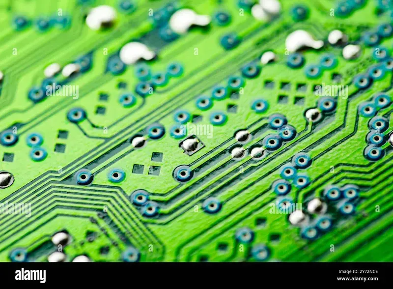
Sensor Node PCB Close-Up
Zero One Solution's Educational Sensor Node PCB Solution is meticulously engineered to address the unique demands of academic and research environments, offering a robust, versatile, and high-performance foundation for a myriad of learning applications. Our design philosophy prioritizes reliability, ease of integration, and efficiency, ensuring that educators and students can focus on innovation rather than technical complexities. This commitment to superior design underpins the advanced capabilities embedded within every PCB we produce for educational sensor nodes, setting a new standard for instructional technology.
Compact Design for Seamless Integration Our PCBs are designed with a remarkably small footprint, enabling them to be easily integrated into various educational projects, from wearable tech for biological studies to miniature environmental monitoring stations. This compact size ensures maximum flexibility without compromising functionality.
Robust Construction for Durability in Learning Environments Understanding the dynamic nature of educational settings, our sensor node PCBs are built with industrial-grade components and undergo rigorous quality control. This robust construction ensures exceptional durability, capable of withstanding frequent handling and diverse operational conditions, thus prolonging the lifespan of educational equipment.
Versatile Multi-Sensor Interface Options A cornerstone of our solution is the comprehensive range of sensor interface options. Our PCBs support a wide array of sensors, including but not limited to, temperature, humidity, light, motion, and gas sensors. This versatility allows for diverse experimental setups, catering to subjects from physics and environmental science to robotics and IoT development.
Optimized for Ultra-Low Power Consumption Recognizing the importance of practical, long-term deployments, our Educational Sensor Node PCBs are meticulously optimized for minimal power draw. This low power consumption significantly extends battery life, enabling extended data collection periods and facilitating autonomous projects without constant recharging, which is crucial for remote monitoring or field studies.
Integrated Wireless Communication Capabilities To facilitate real-time data acquisition and remote monitoring, our PCBs incorporate integrated wireless communication modules such as Bluetooth Low Energy (BLE), Wi-Fi, or LoRa. This feature enables seamless data transmission to computers, mobile devices, or cloud platforms, enhancing the scope of educational projects by allowing students to analyze data remotely.
User-Friendly Debugging and Programming Interfaces Designed with educators and students in mind, our PCBs feature intuitive debugging ports and easy-to-access programming interfaces. This user-centric approach simplifies the development process, accelerates troubleshooting, and empowers students to quickly grasp programming concepts and test their sensor node applications efficiently.
Benefits of Using Our PCB Solution for Educational Purposes
Zero One Solution Limited's PCB solutions provide a transformative advantage for educational sensor node projects, directly addressing common challenges faced by students and educators. Our meticulously engineered PCBs ensure enhanced reliability, reduce prototyping cycles significantly, and offer remarkable cost-effectiveness, all of which culminate in measurably improved student learning outcomes. By streamlining the entire development process for educational initiatives, we empower institutions to focus on innovation and pedagogy rather than technical hurdles.
Enhanced Reliability and Durability Our PCBs are manufactured using high-quality materials and stringent processes, ensuring exceptional reliability and a prolonged operational lifespan. This robustness is critical in educational environments where repeated handling and experimentation are common, minimizing equipment failure and maximizing uninterrupted learning time. Students can confidently iterate and experiment without concerns about component fragility, fostering a more engaging and productive learning experience.
Accelerated Prototyping Cycles Leveraging our rapid prototyping capabilities, educators and students can transform conceptual designs into tangible prototypes at an unprecedented pace. This agility is vital in project-based learning, allowing for quick iteration, testing, and refinement of sensor node designs. Reducing the time from ideation to functional prototype facilitates more comprehensive project exploration within academic timelines, enabling deeper understanding and faster validation of scientific principles.
Cost-Effectiveness for Educational Budgets We understand the budgetary constraints often faced by educational institutions. Our PCB solutions are designed to be cost-effective without compromising on quality or performance. By optimizing material usage and manufacturing efficiency, we provide an economical pathway for schools and universities to equip their labs with advanced sensor node capabilities, making cutting-edge technology accessible to a broader student body and maximizing the return on investment for educational technology.
Improved Student Learning Outcomes The direct and tangible benefits of our PCBs – reliability, speed, and affordability – directly translate into superior educational experiences. Students gain hands-on experience with robust, functional hardware, fostering practical skills in electronics, programming, and data acquisition. This practical engagement enhances theoretical understanding, promotes problem-solving abilities, and prepares students for real-world applications in STEM fields, ultimately leading to more profound and lasting learning outcomes.
Customization Options for Educational Sensor Node PCB Needs
Customizable PCB
For educational institutions, the ability to adapt technology to specific pedagogical goals is paramount. Zero One Solution Limited understands that a one-size-fits-all approach is insufficient for diverse learning environments. Our Educational Sensor Node PCB Solutions offer extensive customization options, empowering educators to tailor their projects precisely to curriculum requirements, student skill levels, and research objectives, thereby maximizing learning impact and practical application.
Flexible Sensor Selection and Integration Educators can choose from a wide array of sensors to integrate into their PCB designs. Whether it's environmental sensors for smart agriculture projects, motion sensors for robotics, or biomedical sensors for health monitoring, our solution accommodates diverse sensor types. We provide design flexibility to ensure seamless integration and optimal performance for various data acquisition needs. This adaptability fosters interdisciplinary learning and allows for the exploration of complex real-world phenomena.
Form Factor Adjustments for Specific Applications The physical dimensions and layout of the sensor node PCB can be customized to fit specific project enclosures, robotic platforms, or experimental setups. From ultra-compact designs for wearable tech to robust, larger boards for outdoor environmental stations, our engineering team works closely with educators to optimize the form factor. This ensures not only functional integrity but also practical usability within the constraints of educational labs and field deployments.
Integration with Existing Educational Platforms and Ecosystems Our customization extends to ensuring compatibility with popular educational platforms such as Arduino, Raspberry Pi, and other microcontrollers commonly used in STEM education. We can design PCBs with specific header pinouts, communication interfaces (e.g., I2C, SPI, UART), and power requirements to seamlessly integrate with pre-existing educational kits and software ecosystems. This reduces the learning curve and allows students to leverage familiar tools while building advanced sensor applications.
Rapid Prototyping: Accelerating Innovation in Education
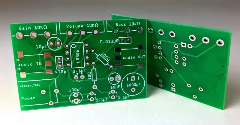
PCB Prototype Sample
Rapid prototyping is a transformative force in educational environments, enabling students and educators to swiftly translate theoretical concepts into tangible, testable hardware. This iterative process is critical for fostering innovation, allowing for quick design iterations, immediate feedback, and accelerated learning cycles in fields like robotics, IoT, and embedded systems. By significantly reducing the time and cost associated with developing and testing sensor node designs, rapid prototyping empowers a more dynamic and engaging educational experience.
Why is rapid prototyping essential for educational sensor node projects? Rapid prototyping is crucial because it allows students to quickly test their designs, identify flaws, and iterate on solutions without significant delays or costs. This hands-on, iterative approach deepens understanding, promotes problem-solving skills, and simulates real-world engineering workflows, where fast cycles are paramount for innovation.
How does Zero One Solution Limited facilitate rapid prototyping for educational PCB solutions? Zero One Solution Limited specializes in rapid-response R&D prototype manufacturing. We achieve this through optimized processes, advanced machinery, and a dedicated team, ensuring fast turnaround times for PCB fabrication and assembly. This allows educational institutions to receive their custom sensor node PCBs quickly, accelerating their project timelines and learning objectives.
What are the advantages of fast turnaround times for educational PCB prototypes? Fast turnaround times enable students to experiment with multiple design iterations within a single academic term, fostering a more agile and comprehensive learning experience. It reduces project bottlenecks, keeps students engaged, and allows for more complex projects to be undertaken, enhancing their practical engineering skills.
Can Zero One Solution Limited handle complex sensor node designs for rapid prototyping? Yes, our extensive experience in rapid prototyping extends to complex designs. We support a wide range of sensor interfaces, component integration, and form factors. Our engineering team can collaborate with educators to optimize designs for manufacturability, ensuring even intricate educational sensor node PCBs are produced efficiently.
Case Studies: Successful Educational Projects Using Our PCBs
Sensor Node Project
Zero One Solution Limited's PCB solutions have been instrumental in empowering numerous educational institutions and research initiatives, enabling students and faculty to bring innovative sensor node projects to fruition. Our robust and customizable PCBs provide the foundational reliability needed for hands-on learning, accelerating the transition from theoretical concepts to practical, real-world applications and fostering a deeper understanding of electronics and data acquisition.
Project Title
Educational Institution
Challenge Addressed
Zero One Solution's Contribution
Impact on Learning/Research
Smart Agriculture Monitoring
University of California, Davis (UCD)
Developing a low-cost, accurate soil moisture and nutrient monitoring system for agricultural research.
Provided custom-designed, compact sensor node PCBs with multiple analog/digital interfaces and low power consumption, optimized for outdoor deployment.
Enabled students to gather real-time agricultural data, leading to a research paper on sustainable farming practices and a deeper understanding of IoT in agriculture. Reduced prototyping time by 40%.
Interactive Environmental Science Kit A high school in Arizona utilized our PCBs to create portable environmental sensor kits for monitoring air quality, temperature, and UV radiation. Our compact and durable PCBs facilitated easy assembly and robust performance in varied field conditions, allowing students to conduct direct environmental impact studies and present data-driven conclusions. This fostered critical thinking and data analysis skills in a practical context.
Robotics Challenge for STEM Students A community college incorporated Zero One Solution's custom sensor node PCBs into their annual robotics competition. These PCBs served as the central hub for various sensors (ultrasonic, IR, accelerometers) on student-designed robots. Our rapid prototyping service allowed students to quickly iterate on their designs, fostering agile development and problem-solving skills under tight deadlines. The reliability of our PCBs ensured that technical failures were minimized, allowing students to focus on algorithmic improvements.
Our Comprehensive Services: From Design to Assembly
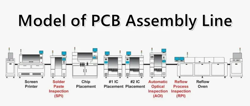
PCB Assembly Line
Zero One Solution Limited offers an unparalleled, integrated suite of services for Educational Sensor Node PCB Solutions, ensuring a seamless journey from initial concept to a fully functional, tested product. Our comprehensive approach streamlines the development process, allowing educators and students to focus on innovation and learning, confident that their hardware foundation is robust and professionally handled.
PCB Design & Optimization Leveraging decades of expertise, our engineers provide meticulous PCB design services tailored for educational sensor nodes, focusing on efficiency, miniaturization, and optimal signal integrity. We ensure designs are robust for hands-on learning and compliant with industry standards, setting students up for success in real-world applications.
Rapid PCB Manufacturing As specialists in rapid prototyping, we accelerate the educational project timeline by providing quick-turn PCB manufacturing. Our advanced facilities handle diverse material requirements and complex layouts, ensuring high-quality boards are produced efficiently to meet tight academic deadlines.
Component Sourcing & Procurement We simplify the complex process of component sourcing by leveraging our extensive global supply chain network. This ensures access to authentic, high-quality electronic components required for educational sensor nodes, minimizing delays and cost overruns, and allowing educators to avoid the complexities of component acquisition.
Precision PCB Assembly (PCBA) Our state-of-the-art assembly lines are equipped for both small-batch educational prototypes and larger-scale project requirements. We employ advanced SMT and THT techniques with stringent quality control, guaranteeing precise component placement and reliable solder joints critical for stable sensor node operation.
Rigorous Testing & Quality Assurance Every assembled Educational Sensor Node PCB undergoes rigorous testing protocols, including electrical testing, functional verification, and environmental stress testing. This meticulous quality assurance process guarantees that each board performs reliably, providing a dependable platform for educational experimentation and research.
Conclusion: Empowering Education Through Innovative PCB Solutions
Zero One Solution Limited's Educational Sensor Node PCB Solution is not merely a product; it is a catalyst for innovation and an enabler of unparalleled learning experiences in modern education. By providing robust, customizable, and rapidly prototyped PCB solutions, we empower students and educators to transform theoretical concepts into tangible, functional projects, thereby deepening understanding and fostering critical problem-solving skills crucial for future technological advancements. Our commitment to excellence and comprehensive, end-to-end services ensures that educational institutions can confidently embark on ambitious sensor node projects, from initial design to final assembly, with a trusted partner by their side.
The intrinsic value of our solution lies in its ability to bridge the gap between classroom theory and real-world application, offering a flexible and reliable foundation for diverse educational initiatives. Whether for environmental monitoring, robotics, IoT development, or interdisciplinary research, our PCBs provide the necessary reliability, performance, and adaptability to meet evolving pedagogical demands. This empowers students to not only understand complex systems but also to actively participate in their creation and optimization.
We invite educators, researchers, and academic institutions to partner with Zero One Solution Limited. Leverage our expertise, rapid prototyping capabilities, and comprehensive PCB services to elevate your educational programs and inspire the next generation of innovators. Together, we can build a future where technological education is more accessible, practical, and impactful, driven by cutting-edge PCB solutions.
In conclusion, Zero One Solution Limited's Educational Sensor Node PCB Solution offers a robust and reliable platform for hands-on learning and experimentation. By providing high-quality PCB design, rapid prototyping, and comprehensive assembly services, we empower educators and students to explore the exciting world of sensor technology. We invite you to contact us today to discuss your specific needs and discover how our expertise can accelerate your educational initiatives. Share this article with your colleagues and let's work together to shape the future of education!