In an era defined by increasing environmental awareness and the pressing need for sustainable practices, the demand for accurate and real-time environmental data has never been greater. Environment monitoring nodes, equipped with sophisticated sensors and robust communication capabilities, play a crucial role in gathering this data. These nodes are the sentinels of our ecosystems, providing insights into air and water quality, soil conditions, and various other environmental parameters. At the heart of every environment monitoring node lies a printed circuit board (PCB), the very foundation upon which all electronic components are mounted and interconnected. A well-designed PCB is paramount to the node's performance, reliability, and longevity. Zero One Solution Limited understands this critical need and provides comprehensive PCB solutions tailored specifically for environment monitoring applications. But what makes a PCB solution ideal for environment monitoring, and how can Zero One Solution Limited help you achieve optimal results? Let's delve into the world of environment monitoring node PCB solutions.
The Importance of PCB Design in Environment Monitoring Nodes
At the heart of every robust environment monitoring node lies a meticulously designed Printed Circuit Board (PCB). A well-engineered PCB is not merely a component; it is the foundational element that dictates the accuracy, reliability, and longevity of the entire monitoring system. Its design profoundly influences how sensitive sensors perform, how efficiently power is managed, and how resilient the node is to harsh environmental conditions, ultimately determining the integrity and trustworthiness of the collected data. For critical applications ranging from industrial safety to climate research, a superior PCB design transitions a theoretical concept into a dependable, real-world solution.
Why is PCB design critical for accuracy in environment monitoring? The accuracy of an environment monitoring node is directly proportional to the integrity of its PCB design. Precision in component placement, meticulous trace routing, and effective electromagnetic interference (EMI) shielding on the PCB are paramount. Any compromise in these areas can introduce noise, signal degradation, or cross-talk, leading to erroneous sensor readings and unreliable data. For instance, in temperature or humidity sensing, even minor signal fluctuations caused by poor PCB layout can result in significant measurement discrepancies, rendering the collected data unusable for critical decision-making.
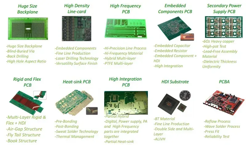
How does PCB design impact the reliability and longevity of monitoring nodes? Reliability and longevity are non-negotiable for environment monitoring nodes, especially those deployed in remote or challenging locations. A well-designed PCB contributes to these aspects by ensuring robust power delivery, thermal management, and mechanical stability. Proper material selection (e.g., FR-4 variants with higher Tg for temperature stability), optimized layer stack-up, and robust solder mask application prevent premature component failure due to heat, vibration, or environmental stressors like humidity and corrosive agents. This meticulous approach ensures the node operates consistently over its intended lifespan, minimizing maintenance and replacement costs.
What role does PCB material selection play in overall system performance? The choice of PCB material is fundamental to the overall performance of an environment monitoring node, particularly when considering the operational environment. Materials like high-Tg FR-4, polyimide, or ceramic substrates offer superior thermal stability and moisture resistance, crucial for nodes exposed to extreme temperatures or high humidity. Dielectric constant and loss tangent are also critical; materials with stable dielectric properties ensure consistent signal propagation, vital for high-frequency sensor communication and data transmission, thereby directly impacting the accuracy and responsiveness of the monitoring system.
How do PCB layout and manufacturing processes affect sensor data integrity? PCB layout and manufacturing processes are pivotal in preserving sensor data integrity. A precise layout minimizes trace lengths, reduces parasitic capacitance and inductance, and isolates sensitive analog signals from noisy digital circuits, thereby preventing signal degradation. Advanced manufacturing processes, including precise etching, accurate drilling, and stringent quality control, ensure that the PCB adheres to the exact design specifications. This precision is vital for maintaining impedance control in high-speed lines and ensuring consistent electrical performance across all circuits, directly translating to clean, accurate, and trustworthy data acquisition from environmental sensors.
Can a poorly designed PCB lead to higher power consumption in monitoring nodes? Absolutely. A poorly designed PCB can significantly increase power consumption in environment monitoring nodes, which is a critical concern for battery-powered or remote applications. Inefficient power routing, inadequate ground planes, and poor component placement can lead to power losses, voltage drops, and increased current draw. For example, long, thin traces can have higher resistance, dissipating more power as heat. Additionally, lack of proper impedance matching can lead to signal reflections and increased power draw in communication circuits. Optimizing the PCB design for power efficiency is crucial for extending battery life and reducing operational costs.
Key Considerations for Environment Monitoring Node PCB Design
Designing Printed Circuit Boards (PCBs) for environment monitoring nodes presents unique challenges, primarily driven by the imperative for robust performance in diverse and often harsh conditions. The criticality of accurate data acquisition, prolonged operational life, and minimal power consumption necessitates a meticulous approach to every design aspect, from component selection to layout strategies. Achieving these objectives requires a deep understanding of the intricate interplay between sensor integration, power efficiency, signal integrity, and the physical protection of the electronics against environmental stressors.
Optimizing Sensor Integration The heterogeneous nature of environmental sensors (e.g., temperature, humidity, air quality, pressure) demands flexible and precise PCB layouts. Key considerations include minimizing trace lengths to reduce signal degradation, implementing proper isolation between analog and digital signals, and ensuring robust power delivery to various sensor types. Calibration requirements and potential electromagnetic interference (EMI) from adjacent components must also be addressed during the design phase to guarantee accurate data readings. For instance, high-precision analog sensors often require dedicated ground planes and shielding to prevent noise coupling from digital circuits, thus preserving measurement accuracy critical for environmental monitoring.
Zero One Solution Limited's Expertise in Environment Monitoring PCB Solutions
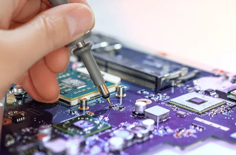
Engineer with PCB Prototype
Zero One Solution Limited stands as a beacon of excellence in providing comprehensive PCB solutions for environment monitoring nodes. Our expertise, honed over a decade in the industry, extends from meticulous design to precision manufacturing and robust assembly, ensuring that every monitoring node functions with unparalleled accuracy and reliability in diverse environmental conditions. We specialize in rapid prototyping, transforming innovative concepts into tangible, high-performance PCBs with exceptional efficiency, crucial for accelerating product development in a fast-paced market.
What distinguishes Zero One Solution Limited's approach to Environment Monitoring Node PCB Solutions? Zero One Solution Limited offers a unique one-stop solution, encompassing PCB design, manufacturing, and assembly under one roof. Our distinct advantage lies in our rapid prototyping capabilities, which significantly reduce development cycles. We integrate deep expertise in sensor integration, power optimization, and signal integrity with a focus on environmental robustness, ensuring solutions are tailored for demanding monitoring applications. Our strategic location in Shenzhen and Dubai provides seamless access to global supply chains and a competitive edge in material sourcing and production efficiency, resulting in superior product performance and faster market entry for our clients' environment monitoring nodes.
Service Aspect
Zero One Solution Limited's Advantage
Benefit for Environment Monitoring Nodes
PCB Design & Layout
Expertise in sensor integration, low-power design, and robust signal integrity for accurate data acquisition.
Ensures high precision and reliability of sensor readings, critical for sensitive environmental data.
Rapid Prototyping
Accelerated development cycles (days instead of weeks), facilitating quicker iteration and testing.
Significantly reduces time-to-market for new environmental monitoring products and innovations.
Manufacturing & Assembly
Advanced facilities, stringent quality control, and specialized processes for harsh environment compatibility.
Guarantees long-term operational stability and durability of monitoring nodes in challenging conditions.
Material Selection for Harsh Environments
PCB Material Selection
For environment monitoring nodes deployed in challenging conditions, the choice of PCB materials is not merely a design consideration but a critical determinant of system longevity, accuracy, and operational reliability. Harsh environments, ranging from extreme temperatures and high humidity to corrosive chemical exposure and mechanical stress, demand materials that can maintain their electrical and mechanical integrity over prolonged periods. Selecting the right substrate, laminate, and finish is paramount to prevent failures such as delamination, signal degradation, or short circuits, thereby ensuring the continuous and precise operation of monitoring equipment in critical applications.
Material Type
Key Properties
Typical Applications in Environment Monitoring
FR-4 (Standard)
Good electrical properties, cost-effective, widely available
Indoor, controlled environments (e.g., office air quality monitoring)
Why is material selection critical for Environment Monitoring Node PCB Solutions? The operational environment directly impacts the PCB's performance and lifespan. Materials must withstand specific stressors like extreme temperatures (hot/cold), high humidity, corrosive elements, UV radiation, and vibrations. Inadequate material selection can lead to irreversible damage, affecting sensor accuracy, power integrity, and communication reliability, ultimately causing system failure and data loss. For instance, standard FR-4 might absorb moisture in humid environments, leading to decreased insulation resistance and signal integrity issues, while specialized materials like PTFE are designed to resist such conditions effectively.
Optimizing Power Management on the PCB
Optimized Power Management PCB
For environment monitoring nodes, particularly those deployed in remote or hard-to-reach locations, optimizing power management on the PCB is not merely a design choice but a critical determinant of operational longevity and cost-effectiveness. A meticulously engineered power management system on the PCB ensures that the node can operate autonomously for extended periods, directly impacting the feasibility and reliability of long-term data collection without frequent battery replacements or external power sources.
Component Selection for Energy Efficiency The foundation of an energy-efficient environment monitoring node PCB lies in the judicious selection of components. Prioritize microcontrollers (MCUs) with low-power modes (e.g., sleep, deep sleep, hibernate) and efficient wake-up mechanisms, such as those based on ARM Cortex-M series or specialized ultra-low-power MCUs. Similarly, select sensors, communication modules (e.g., LoRa, NB-IoT, BLE), and voltage regulators (LDOs, DC-DC converters) that boast industry-leading quiescent current (Iq) ratings and high conversion efficiencies. For instance, a DC-DC converter with 95% efficiency significantly outperforms one with 80% efficiency over the long term, reducing heat dissipation and extending battery life. Always refer to manufacturer datasheets for precise power consumption figures under various operating conditions and evaluate trade-offs between performance and power.
Power Management Technique
Description
Impact on Node Operation
Zero One Solution Approach
Low-Power Mode Implementation
Utilizing MCU sleep/deep sleep states, waking only for data acquisition or transmission events.
Significantly extends battery life; crucial for remote deployments.
Strategic selection of ultra-low-power MCUs and firmware-level power state management expertise for optimal duty cycling.
Efficient Power Routing and Layout Beyond component selection, intelligent power routing and PCB layout are paramount. Minimize trace lengths for power lines to reduce resistive losses (I²R losses), especially for higher current paths. Employ wider traces for power and ground planes to reduce impedance and ensure stable voltage delivery. Implement proper decoupling capacitance near power pins of ICs to filter noise and provide instantaneous current. Grouping analog and digital grounds appropriately and using star topology for critical power rails can prevent ground loops and reduce noise. Additionally, consider the thermal management aspects of power components to ensure their optimal efficiency and longevity, as excessive heat can degrade performance and increase power consumption.
Power Management Technique
Description
Impact on Node Operation
Zero One Solution Approach
Voltage Regulation Optimization
Employing highly efficient LDOs or DC-DC converters tailored to specific voltage requirements and load profiles.
Minimizes energy waste during voltage conversion, vital for varying loads.
Expertise in selecting and integrating high-efficiency power converters, considering input/output voltage ranges and current demands.
What are the primary power consumption culprits in an environment monitoring node? The primary power consumption culprits in an environment monitoring node typically include the microcontroller (MCU) during active processing, sensor operation and data acquisition, and especially the wireless communication module during data transmission. The frequency and duration of these active states significantly dictate overall power draw, making duty cycling a crucial optimization strategy. Inefficient voltage regulators and parasitic currents from poorly designed layouts can also contribute substantially to power loss.
Ensuring Signal Integrity for Accurate Data Acquisition
Signal Integrity Testing
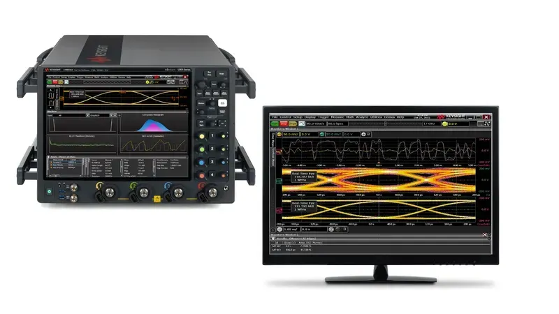
Accurate data acquisition from environmental sensors is paramount for effective environment monitoring. The integrity of signals transmitted across the PCB directly impacts the reliability and precision of collected data. Signal integrity (SI) is a critical design consideration, as even minor noise or interference can corrupt sensor readings, leading to erroneous interpretations and potentially flawed environmental assessments. Achieving robust SI involves meticulous PCB layout, strategic component placement, and the application of proven electromagnetic compatibility (EMC) techniques to minimize signal degradation and external interference.
How does impedance matching improve signal integrity in environment monitoring PCBs? Impedance matching ensures that the impedance of the transmission line (PCB trace) closely matches the impedance of the source and load. Mismatched impedances cause signal reflections, leading to signal distortion and loss, particularly at higher frequencies. For accurate sensor data, impedance matching minimizes these reflections, preserving signal shape and amplitude, which is crucial for precise analog sensor readings and reliable digital communication within the environment monitoring node.
What are the most effective grounding techniques for noise reduction in sensitive environmental sensor circuits? Effective grounding is fundamental for noise reduction. Star grounding, where all ground connections radiate from a single point, minimizes ground loops and common-mode noise. Dedicated analog and digital ground planes, connected at a single point, prevent noise from digital circuits from affecting sensitive analog sensor signals. Furthermore, using a solid ground plane across the PCB provides a low-impedance return path for signals and acts as a shield against electromagnetic interference, enhancing the signal-to-noise ratio for accurate data acquisition in environment monitoring nodes.
Zero One Solution Limited employs advanced design practices and simulation tools to rigorously analyze and optimize signal integrity on our environment monitoring node PCBs. Our expertise ensures that critical sensor data remains uncompromised, even in challenging operational environments, directly contributing to the accuracy and reliability of your environmental monitoring solutions. Our one-stop service from design to manufacturing guarantees that these meticulous SI considerations are faithfully translated into the final product.
SI Challenge
Description
PCB Design Solution
Crosstalk
Unwanted coupling of energy between adjacent traces.
Increasing trace spacing, using guard traces, orthogonal routing on adjacent layers, differential pairs for high-speed signals
Ripple and fluctuations in the power rails affecting sensitive circuits.
Effective power plane design, optimal placement of bypass and decoupling capacitors, using low-ESR capacitors
PCB Assembly and Testing for Reliability in Environment Monitoring Nodes
PCB Assembly and Testing
Ensuring the long-term reliability and accurate performance of environment monitoring nodes hinges critically on meticulous PCB assembly and rigorous testing protocols. Even the most impeccably designed PCB can fail if assembly introduces flaws or if inadequate testing overlooks latent defects, compromising data integrity and operational longevity in often challenging deployment environments. Zero One Solution Limited prioritizes a comprehensive quality assurance framework throughout the assembly and testing phases to deliver highly dependable Environment Monitoring Node PCB Solutions.
Why is proper PCB assembly crucial for environment monitoring nodes? Proper PCB assembly is vital because environment monitoring nodes often operate in remote, harsh, or inaccessible locations where failures are costly and difficult to rectify. High-quality assembly ensures robust physical connections, optimal thermal management, and reliable electrical pathways, all of which are essential for the continuous and accurate operation of sensors and communication modules over extended periods. Substandard assembly can lead to intermittent failures, data inaccuracies, or complete system shutdowns, negating the purpose of the monitoring node.
What specific testing procedures are essential for Environment Monitoring Node PCBs? Essential testing procedures include In-Circuit Testing (ICT) to verify component placement and solder joint integrity, Functional Testing (FCT) to simulate operational conditions and validate sensor accuracy and data transmission, and Environmental Stress Screening (ESS) such as thermal cycling and humidity testing to expose potential weaknesses under simulated environmental extremes. Additionally, burn-in testing can identify early-life failures, ensuring only robust PCBs are deployed, critical for applications where field repairs are impractical.
How does Zero One Solution Limited ensure the quality of PCB assembly for environmental applications? Zero One Solution Limited employs advanced automated assembly lines, including high-precision pick-and-place machines and automated optical inspection (AOI), to minimize human error and ensure consistent quality. Our processes adhere to IPC standards (e.g., IPC-A-610 Class 2 or 3 for high-reliability applications), and we implement stringent quality control checks at every stage, from solder paste inspection (SPI) to X-ray inspection (AXI) for complex components like BGAs. This meticulous approach guarantees the integrity of every solder joint and component placement.
What role does comprehensive testing play in the long-term performance of monitoring nodes? Comprehensive testing plays a paramount role in predicting and preventing field failures, thus extending the operational lifespan and ensuring the long-term, uninterrupted performance of environment monitoring nodes. By rigorously testing under conditions mimicking actual deployment, potential issues related to temperature variations, vibrations, or power fluctuations are identified and rectified before the product reaches the field. This proactive approach significantly reduces warranty claims and maintenance costs, bolstering confidence in the deployed system's reliability.
Can Zero One Solution Limited provide custom testing solutions for unique environmental monitoring requirements? Yes, Zero One Solution Limited specializes in providing tailored testing solutions to meet the unique and specific requirements of various environmental monitoring applications. We work closely with clients to understand their exact operational environments, sensor types, and data transmission protocols. Based on this, we can develop custom test fixtures, write specific test scripts, and implement specialized environmental simulations (e.g., salt spray tests for marine environments or vibration tests for vehicle-mounted nodes) to ensure the PCB's performance meets all necessary standards and withstands anticipated challenges.
Case Studies: Successful Environment Monitoring Node PCB Projects
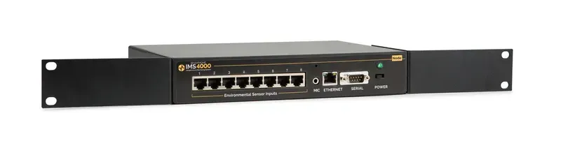
Environment Monitoring Node Device
Real-world case studies demonstrate the tangible impact of optimized PCB solutions in delivering robust and reliable environment monitoring nodes. These examples highlight how Zero One Solution Limited's expertise translates into superior performance, extended operational life, and cost-efficiency for diverse environmental applications, showcasing our commitment to solving complex engineering challenges through precision PCB design, manufacturing, and assembly.
Project Type
Challenge Addressed
Zero One Solution
Key Benefit Achieved
Remote Agricultural Sensor Node
Extreme temperature fluctuations and high humidity required robust PCB substrate and conformal coating.
Utilized high-Tg FR-4 material with a specialized hydrophobic coating; optimized component placement for thermal dissipation.
Increased sensor lifespan by 40% and maintained data accuracy across varied weather conditions, reducing maintenance costs significantly.
Project Type
Challenge Addressed
Zero One Solution
Key Benefit Achieved
Urban Air Quality Monitoring Station
Miniaturization and high-density sensor integration with low power consumption for continuous operation.
Implemented multi-layer PCB design with optimized trace routing for minimal EMI; integrated custom power management unit for efficient energy harvesting.
Achieved a 30% reduction in PCB footprint, enabling compact device deployment, and extended battery life by 25% for prolonged monitoring intervals.
Project Type
Challenge Addressed
Zero One Solution
Key Benefit Achieved
Industrial Wastewater Quality Probe
Corrosive chemical exposure and demanding signal integrity for electrochemical sensors.
Selected chemical-resistant PCB materials (e.g., polyimide) and employed differential pair routing for sensitive analog signals; applied robust hermetic sealing.
Ensured precise sensor readings in harsh chemical environments, enhancing regulatory compliance and preventing costly equipment failures due to inaccurate data.
Project Type
Challenge Addressed
Zero One Solution
Key Benefit Achieved
Wildlife Tracking Collar (Biomonitoring)
Ultra-low power consumption and durability in rough outdoor terrains; GPS and various bio-sensors integration.
Designed a flexible PCB for compact form factor and impact resistance; optimized power rails for various sleep modes and efficient energy harvesting.
Extended operational time between charges by 50%, allowing for longer monitoring periods and more comprehensive data collection on animal behavior.
How does Zero One Solution Limited ensure PCB reliability in harsh environments? We employ a multi-faceted approach, including selecting specialized PCB substrates (e.g., high-Tg, low Dk/Df, or flexible materials), applying robust conformal coatings or encapsulations, and optimizing component placement for thermal management. Our rigorous testing protocols, including environmental stress screening (ESS) and highly accelerated life testing (HALT), simulate extreme conditions to ensure long-term reliability and performance in even the most challenging environments.
Future Trends in Environment Monitoring PCB Technology
The landscape of Environment Monitoring Node PCB technology is constantly evolving, driven by the demand for more compact, efficient, and interconnected devices. Future trends are largely focused on enhancing data acquisition capabilities, extending operational lifespans, and enabling seamless integration into broader IoT ecosystems. These advancements in PCB design and manufacturing are pivotal for creating the next generation of environmental sensors that are not only more accurate but also more adaptable to diverse deployment scenarios.
How will flexible PCBs impact future environment monitoring nodes? Flexible PCBs (FPCBs) will revolutionize environment monitoring nodes by enabling highly conformable and lightweight designs. Their ability to bend and twist allows for deployment in irregular spaces or integration directly into wearable or uniquely shaped environmental sensors, where rigid PCBs are impractical. This flexibility reduces overall device size and weight, improves shock resistance, and opens up new possibilities for distributed sensing networks, ultimately leading to more pervasive and less obtrusive monitoring solutions. This technology also facilitates the integration of more sensors and components within a smaller footprint, enhancing the node's data collection capabilities while maintaining a compact form factor for easier deployment in varied environments like smart agriculture or infrastructure monitoring where space constraints are critical.
What role does miniaturization play in the evolution of environment monitoring PCBs? Miniaturization is a critical trend for environment monitoring PCBs, enabling the creation of smaller, more discreet, and power-efficient nodes. This involves the use of smaller components (e.g., 0201 or 01005 packages), higher-density interconnects (HDIs), and advanced substrate materials. Miniaturization allows for the deployment of multiple sensors in a tight space, facilitates integration into existing infrastructure, and reduces the environmental footprint of the devices. It also supports the development of self-powered or energy-harvesting nodes, as smaller components often require less power, extending battery life and reducing maintenance needs in remote locations. This trend is crucial for applications like air quality monitoring in urban areas or water quality assessment in sensitive ecosystems, where unobtrusive and long-lasting solutions are paramount, allowing for a higher density of monitoring points and more granular data collection without visual intrusion.
How is wireless communication integration changing environment monitoring PCB design? Wireless communication integration is profoundly changing environment monitoring PCB design by making nodes more versatile and easier to deploy without the need for extensive cabling infrastructure. The integration of modules for technologies like LoRaWAN, NB-IoT, 5G, Wi-Fi, and Bluetooth Low Energy (BLE) directly onto the PCB streamlines data transmission to cloud platforms or central hubs. This trend necessitates careful consideration of antenna design, RF shielding, and power efficiency on the PCB to ensure reliable long-range communication while minimizing power consumption. The shift towards integrated wireless capabilities simplifies installation, reduces costs, and expands the deployment possibilities for environmental monitoring, especially in remote or inaccessible areas where wired connections are not feasible. This also supports real-time data streaming, enabling immediate alerts and proactive responses to environmental changes, which is vital for applications like early warning systems for natural disasters or industrial leak detection.
In conclusion, the effectiveness of environment monitoring nodes hinges significantly on the quality and design of their PCBs. Zero One Solution Limited offers comprehensive PCB solutions, from design to manufacturing and assembly, tailored to meet the unique demands of environmental monitoring applications. By leveraging our expertise, you can ensure the reliability, accuracy, and longevity of your monitoring systems, contributing to a healthier and more sustainable future. Contact Zero One Solution Limited today to discuss your environment monitoring node PCB needs and discover how we can help you achieve your project goals. Let's work together to build a smarter, more sustainable world, one PCB at a time.