
In the hyper-competitive world of vaping hardware, the gap between a successful prototype and a profitable product launch is the DFM process. Micro PCBA design presents unique challenges, where miniaturization meets stringent reliability requirements. This guide empowers engineers to navigate the complexities of manufacturing, ensuring your design is built for speed, quality, and scale.
The Anatomy of Micro PCBA for Vaping Hardware
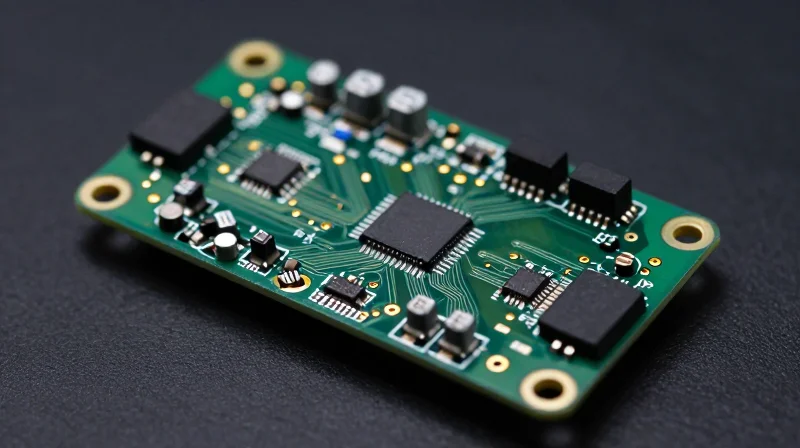
At the heart of every modern electronic cigarette lies a micro Printed Circuit Board Assembly (PCBA) engineered to operate within a highly compressed form factor. Unlike standard industrial electronics, vaping hardware requires a design architecture that integrates battery management, sensor feedback, and atomizer regulation onto a substrate often smaller than a standard postage stamp. Achieving reliability in this space requires a holistic approach to component placement, thermal management, and structural integrity.
Key Micro PCBA Architecture Challenges
| Design Constraint | Technical Impact | Mitigation Strategy |
|---|---|---|
| Spatial Volume | Component crowding increases signal noise. | Utilize 0201 or 01005 passives. |
| Thermal Density | Excess heat degrades MCU performance. | Strategic copper pouring and thermal vias. |
| Regulatory Compliance | Lead-free mandates affect solder reliability. | Utilize high-Tg laminates for durability. |
Fundamental Components of a Vaping PCBA
The micro PCBA typically functions as the brain of the device, coordinating energy transfer from the lithium-ion cell to the heating coil. Designers must prioritize power-efficient MOSFETs, low-latency microcontrollers, and precision sensors (such as pressure or airflow sensors) to ensure a consistent user experience while meeting strict safety standards.
- Why is micro-miniaturization critical for vaping?
Vaping devices are consumer handhelds where aesthetic portability is paramount; the PCBA must fit within a restricted chassis without sacrificing battery capacity or heating performance. - How does moisture ingress affect micro PCBA design?
Condensation from aerosolized liquids can cause short circuits; therefore, conformal coating and hermetic sealing strategies must be integrated directly into the PCBA layout phase. - What is the primary DFM focus for micro-vaping boards?
The focus is on optimizing trace routing to minimize EMI while ensuring that assembly houses can maintain high-yield SMT throughput despite the extreme component density.
Optimizing Copper Weight for High-Current Demands
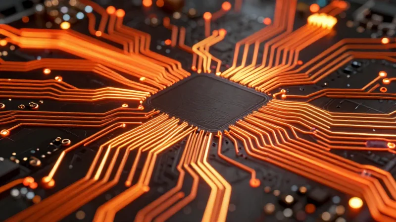
Balancing Current Density and Thermal Limits
In the confined architecture of a vape device, high current discharge from lithium-ion cells poses significant thermal risks to the PCB. Designers must move beyond standard 1oz copper specifications, utilizing advanced PCB calculators to determine the minimum cross-sectional area required to keep temperature rise within safe operating limits, typically defined as under 10°C above ambient for these compact units.
Comparison of Copper Weight Configurations
| Copper Weight | Current Capacity | Recommended Application | Manufacturing Complexity |
|---|---|---|---|
| 0.5 oz (17.5µm) | Low | Logic & Sensor Circuits | Low |
| 1.0 oz (35µm) | Moderate | Standard Power Paths | Low |
| 2.0 oz (70µm) | High | Main Discharge Paths | Medium |
Strategic Layout Techniques for Thermal Management
Simply increasing copper weight is often insufficient if the PCB layout does not account for heat dissipation. Designers should utilize short, wide traces for high-current paths and implement thermal relief patterns where copper connects to large surface mount pads. Furthermore, employing internal copper planes can serve as a heat sink, effectively drawing thermal energy away from sensitive components like MOSFETs and microcontrollers.
Frequently Asked Questions
- Can I use thinner copper to save space?
Yes, but you must compensate with wider traces. If spatial constraints prevent wide traces, thicker copper (2oz+) is necessary to avoid overheating during high-wattage puffs. - How does PCB plating thickness affect resistance?
Total resistance is inversely proportional to copper thickness. Increased plating thickness reduces DC resistance, leading to less power loss as heat across the board.
Advanced Thermal Management Strategies
Advanced Thermal Management Strategies
In the confined architecture of a micro vaping PCBA, thermal density is the primary limiting factor for battery cycle life and component longevity. As devices shift toward sub-ohm performance and higher power outputs, simple copper pours are no longer sufficient. Engineers must implement holistic thermal management that prioritizes low-resistance heat paths from the MOSFETs and microcontroller units (MCUs) to the chassis or external housing, treating the entire enclosure as an active heat sink.
Via-in-Pad and Thermal Relief Best Practices
Thermal vias serve as the primary conduction bridge between internal layers and external heat spreaders. Utilizing via-in-pad technology allows for direct thermal transfer from high-power components, but it mandates strict assembly oversight to prevent solder wicking and joint starvation.
| Technique | Primary Advantage | DFM Consideration |
|---|---|---|
| Via-in-Pad | Shortest thermal path to ground plane | Requires conductive epoxy or capping/plating |
| Thermal Relief | Prevents soldering cold joints | Balance relief width vs. current carrying capacity |
| Heat-Conductive Potting | Uniform heat distribution | Increases total mass and assembly time |
- How do I optimize via spacing for heat?
Maintain a pitch of 0.8mm to 1.2mm between thermal vias. Reducing pitch below 0.5mm risks compromising the mechanical integrity of the PCB base material during the reflow cycle. - When should thermal relief be avoided?
On high-current paths, thermal relief spokes act as bottlenecks. If the component operates under sustained high thermal stress, use a solid copper connection and increase the soldering process temperature to ensure complete wetting. - What is the role of the housing interface?
For optimal cooling, ensure the design incorporates a mechanical landing pad on the PCB that aligns with a high-thermal-conductivity silicone pad placed between the board and the device chassis.
Selecting the Right Substrate for Reliability
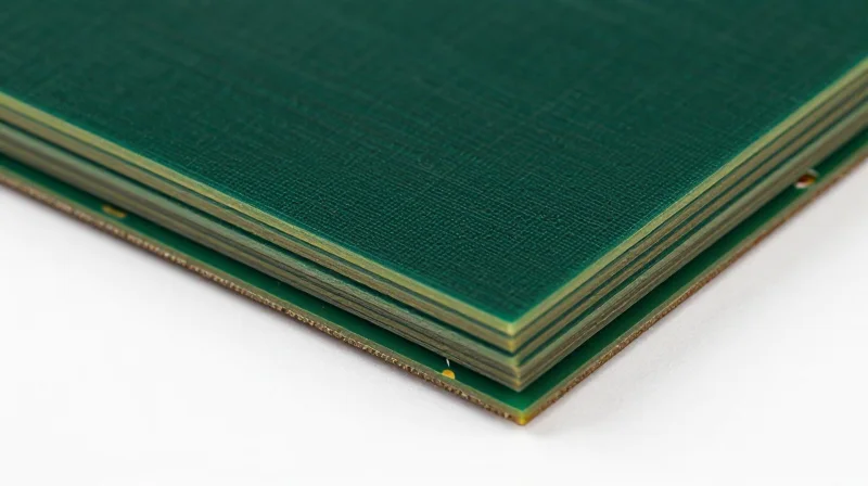
Substrate Material Selection Criteria
The performance of a micro PCBA within an electronic cigarette is fundamentally dictated by the laminate's ability to maintain mechanical integrity under continuous thermal cycling. Standard FR4 is often insufficient due to the localized heat generated by high-discharge lithium-ion batteries and heating elements. Designers must prioritize substrates with high Glass Transition Temperatures (Tg) and low Coefficient of Thermal Expansion (CTE) to prevent delamination, pad lifting, and conductive anodic filament (CAF) growth.
| Material Type | Key Advantage | Primary Application |
|---|---|---|
| Standard FR4 | Cost-effective | Simple, low-power control boards |
| High-Tg FR4 | Thermal stability >170°C | High-drain pods and mod circuits |
| Polyimide | Extreme flexibility & heat resistance | Compact flex-rigid connectors |
Mitigating Thermal Fatigue
To achieve long-term reliability, the substrate must match the Z-axis expansion of the copper features. Mismatched expansion rates during the heating and cooling phases of a vaping session place extreme stress on barrel vias, often leading to micro-cracking. Utilizing high-Tg materials ensures that the substrate remains in a glassy, rigid state even at peak operating temperatures, effectively stabilizing the structural interconnections.
- Why is Tg critical for e-cigarette PCBs?
A high Tg prevents the substrate from transitioning into a rubbery state during use, which maintains the integrity of high-density interconnects and prevents board warping. - Is Polyimide necessary for all micro designs?
No; while Polyimide offers superior heat resistance, its cost is higher. It should be reserved for areas requiring extreme bending radii or specific high-heat zones near the atomizer connection. - How does moisture impact substrate choice?
Electronic cigarettes are susceptible to e-liquid seepage; choosing substrates with low moisture absorption properties reduces the risk of electrical shorts and electrolytic migration over time.
Precision Component Placement and SMT Yield

Optimizing Placement Precision for Micro-Scale Assemblies
Achieving high yields in the assembly of ultra-compact electronic cigarette PCBA requires an uncompromising approach to machine vision and mechanical alignment. Because components are often scaled down to 0201 or 01005 metric sizes, standard assembly tolerances are insufficient. Design engineers must integrate global and local fiducial markers to allow for automated optical inspection (AOI) and precise reference point calibration. By minimizing the distance between the center of gravity of the component and the pick-up site, and by utilizing high-accuracy fiducials, manufacturers can significantly reduce the risk of tombstoning and misaligned solder joints.
Stencil and Solder Paste Control
The stencil design for micro-PCBA requires a meticulous aperture-to-pad ratio. Laser-cut stainless steel stencils with electro-polishing are mandatory to ensure consistent paste release in miniaturized geometries. Oversizing apertures can cause bridging, while undersizing leads to insufficient solder volume, creating cold joints during high-current battery pulses.
| Parameter | Micro-PCBA Requirement | Justification |
|---|---|---|
| Fiducial Size | 0.5mm - 1.0mm | Ensure vision system clarity |
| Paste Thickness | 0.08mm - 0.1mm | Avoids bridging on fine pitch |
| Component Spacing | Min 0.2mm | Prevent cross-contamination |
Manufacturing Reliability FAQs
- How do fiducial markers impact placement accuracy?
Local fiducials placed directly adjacent to fine-pitch micro-components allow the pick-and-place machine to perform real-time offset corrections, mitigating thermal expansion errors inherent in compact board layouts. - Can solder mask defined pads help with yield?
Yes, for 0201 and smaller components, using Solder Mask Defined (SMD) pads provides superior registration and prevents the pad from lifting during the high-heat cycles typical of vape device operation. - Why is stencil nano-coating recommended?
Nano-coatings reduce solder paste accumulation on the underside of the stencil, minimizing the frequency of manual cleaning cycles and preventing solder smearing on high-density micro-PCBA surfaces.
DFM and Regulatory Testing Requirements
Aligning DFM with Regulatory Standards
Regulatory agencies, including the FDA and CE, mandate stringent testing for battery management systems and heating element controllers. By designing boards with test points located in non-critical electrical paths and utilizing clean-room standard soldering processes, manufacturers reduce the risk of ionic contamination—a major cause of board failure under regulatory scrutiny.
Key Regulatory and Testing Benchmarks
| Requirement Category | Design Consideration | Compliance Impact |
|---|---|---|
| Material Safety | Halogen-free PCBs | RoHS & REACH compliance |
| Thermal Integrity | Controlled impedance | Safety for high-discharge cells |
| Moisture/Vapor | Conformal coating access | Corrosion prevention under IP ratings |
Frequently Asked Questions on Compliance
- How does DFM affect UL certification timelines?
Implementing standardized clearances and utilizing recognized flame-retardant substrates (UL 94V-0) significantly reduces the time required for electrical safety evaluations. - Why is traceability critical in PCBA DFM?
Regulatory bodies require full batch traceability; integrating high-resolution laser-etched serial numbers on the PCBA silk screen during the design phase ensures seamless auditability. - What role does testing play in design verification?
Design for Testing (DFT) features, such as integrated test pads for in-circuit testing (ICT), allow for rapid verification of battery protection circuit activation thresholds without manual rework.
Manufacturers should prioritize early-stage environmental stress screening (ESS). By designing the PCBA to withstand vibration and thermal shock testing protocols as defined by ISO standards, companies minimize the need for design iterations post-certification, ultimately accelerating time-to-market.
Streamlining the Prototype-to-Production Transition
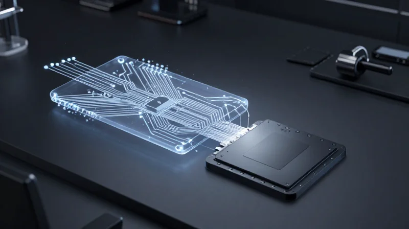
Synchronizing Design Intent with Manufacturing Capability
The transition from a functional prototype to a high-volume micro PCBA relies on the seamless communication of engineering constraints to the shop floor. Discrepancies between CAD data and factory equipment capabilities often lead to yield degradation. Designers must mandate early involvement of process engineers to validate stack-up feasibility and panelization strategies before the design is frozen.
Standardizing the Handoff Process
| Transition Phase | Common Bottleneck | DFM Mitigation Strategy |
|---|---|---|
| Pre-Production | DNP/BOM conflicts | Unified cloud-based BOM management |
| NPI Phase | Reflow profile drift | Instrumented test-coupon validation |
| Full Assembly | Fiducial recognition errors | Standardized optical alignment patterns |
Addressing Transition FAQ
- Why does my prototype pass SMT but fail at scale?
Prototype builds often rely on manual intervention or lenient process windows. Scaling requires rigorous adherence to IPC-Class II or III standards, ensuring that micro-vias and tight trace-to-pad clearances are optimized for automated solder paste inspection (SPI) and AOI. - How can I reduce NPI cycles?
Implement 'Design for Manufacturing' reviews at the 30% and 70% design completion stages. By identifying tooling limitations, such as board thickness constraints or stencil aperture requirements early, you prevent multiple respins. - Is data-driven feedback essential?
Yes. Integrating automated test data from the production line back into the CAD environment allows engineers to tighten design tolerances specifically where process variations occur, directly increasing assembly yield.
Automating Design Rule Verification
def validate_production_readiness(board_metrics):
    if board_metrics['fiducials'] < 3:
        raise ValueError('Insufficient fiducial count for automated SMT.')
    if board_metrics['pad_clearance'] < 0.15:
        return 'Warning: Tight clearance, verify solder mask dam capability.'
    return 'Ready for production batching.'
By mastering these DFM principles, you mitigate production risks and ensure your product delivers a consistent, safe experience for your users. Don't let design oversights derail your production timeline. Contact our engineering team today for a comprehensive DFM audit of your latest vaping hardware design.
