In our interconnected world, advanced electronics are powered by increasingly complex circuit boards. The 8-layer PCB, a workhorse for many sophisticated devices, requires precision and expertise in manufacturing. Much like a well-orchestrated symphony relies on each instrument, an efficient 8-layer PCB ensures harmonious functioning in critical applications. This guide serves as a beacon to navigate the landscape of 8 layer PCB manufacturers, ensuring you select a partner who understands your intricate needs.
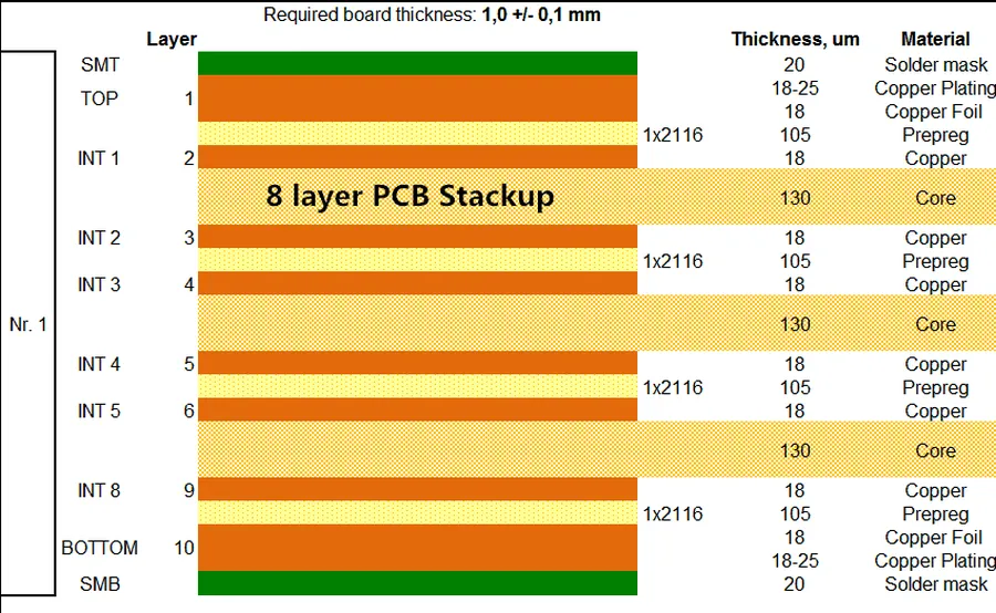
An 8-layer printed circuit board (PCB) is a sophisticated multi-layer structure, characterized by eight conductive layers of copper circuitry embedded within a stack of insulating substrate material. These boards offer a significant leap in complexity and performance compared to single or double-layer designs, enabling advanced electronic functionality. The increased layer count allows for enhanced routing flexibility, improved signal integrity, and greater component density.
| Feature | Single-Layer PCB | Double-Layer PCB | 8-Layer PCB |
|---|---|---|---|
| Number of Conductive Layers | 1 | 2 | 8 |
| Routing Flexibility | Limited | Moderate | High |
| Signal Integrity | Low | Moderate | High |
| Component Density | Low | Moderate | High |
| Complexity | Low | Medium | High |
| Cost | Low | Medium | High |
| Typical Applications | Simple Electronics | Consumer Electronics | Industrial, Medical, Aerospace |
The complexity of an 8-layer PCB introduces new design considerations, necessitating advanced engineering techniques for optimal performance. These include precise impedance control, meticulous layer stackup to mitigate noise, and thorough thermal management to ensure reliability. Common applications of 8-layer PCBs include: * **Industrial Automation:** High-precision control systems, robotics, and sensor networks demand sophisticated circuitry. * **Medical Devices:** Imaging equipment, patient monitoring systems, and diagnostic tools benefit from enhanced signal integrity and compact form factors. * **Telecommunications:** Networking infrastructure, high-speed data transmission, and signal processing require complex routing and minimal interference. * **Aerospace and Defense:** Avionics, radar systems, and satellite communications rely on robust performance under extreme conditions. * **High-Performance Computing:** Servers, data centers, and advanced processors leverage increased signal density and thermal control for advanced applications. * **Advanced Consumer Electronics**: High-end smartphones, gaming consoles, and virtual reality headsets use 8-layer PCBs to manage complex integrated circuits and high-speed data transfer.
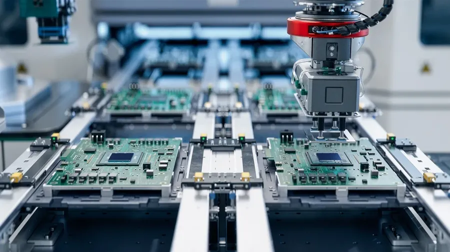
Selecting the right 8-layer PCB manufacturer is crucial for the success of any electronic product that relies on high-performance multilayer boards. This section delves into the essential factors to consider, ensuring the chosen partner can meet specific project requirements, from design complexity to final quality and reliability.
The selection process should encompass a thorough evaluation of the manufacturer's capabilities, materials, certifications and quality control processes, and lead time management. Each aspect directly influences the performance, reliability, and overall cost of the final product.
| Factor | Description | Importance |
|---|---|---|
| Manufacturing Capabilities | Ability to produce specified trace widths, spacing, hole diameters, and via types. | Critical for achieving the desired electrical performance and design density. |
| Material Selection | Options for base materials (e.g., FR-4, high-Tg FR-4) and prepreg materials. | Affects thermal performance, signal integrity, and overall board reliability. |
| Certifications | Compliance with industry standards such as ISO 9001, UL, IPC standards. | Ensures the manufacturer adheres to established quality and safety guidelines. |
| Quality Control Processes | Implementation of rigorous testing, including AOI, electrical tests, and functional tests. | Minimizes defects and enhances overall product quality and reliability. |
| Lead Times | Expected duration from design submission to board delivery. | Directly impacts project timelines and production schedules. Shorter lead times can be advantageous, but should not compromise quality. |
| Production Processes | Understanding of each step in the production process, from design review to final testing. | Ensure consistent quality and allow proper integration with the overall project pipeline. |
Selecting the right 8-layer PCB manufacturer is crucial for project success. This section offers a comparative analysis of leading manufacturers based on their expertise, technological capabilities, customer feedback, and pricing structures, aiming to streamline the selection process for our readers.
| Manufacturer | Expertise | Technology | Customer Feedback | Pricing | Typical Lead Time |
|---|---|---|---|---|---|
| Manufacturer A | High reliability boards, complex designs | Advanced HDI, fine-line etching, controlled impedance | Positive, responsive customer service, good for prototyping | Premium, higher for lower volumes | 2-4 weeks |
| Manufacturer B | Large volume production, cost effective solutions | Automated lines, standard material selections, wide range of surface finishes | Consistent quality, good for large orders, slightly slower response | Competitive, scalable pricing | 3-5 weeks |
| Manufacturer C | Specialized in high-speed boards, RF applications | Low-loss laminates, high-precision fabrication, advanced testing capabilities | Highly skilled engineering support, preferred for specialist requirements | High, best for specific material or precision needs | 4-6 weeks |
| Manufacturer D | Fast turnaround prototyping, low to medium volumes | Quick-turn capabilities, online quoting and ordering platforms | Good communication, ideal for iterating designs, occasional tolerance issues | Moderate, balanced pricing for prototypes | 1-3 weeks |
| Manufacturer E | General purpose boards, consistent quality, good all rounder | Established technologies, wide range of sizes, standard PCB manufacturing process | Good support, suitable for many applications, can get busy | Moderate, fair prices | 2-4 weeks |
Note: This table provides a general overview. Specific project needs may dictate the most suitable manufacturer. It is recommended to reach out to several manufacturers to compare detailed quotations and samples to ensure optimal project fit. The typical lead times listed may vary based on specific board design and volume requirements. Pricing can vary drastically depending on project specifications.
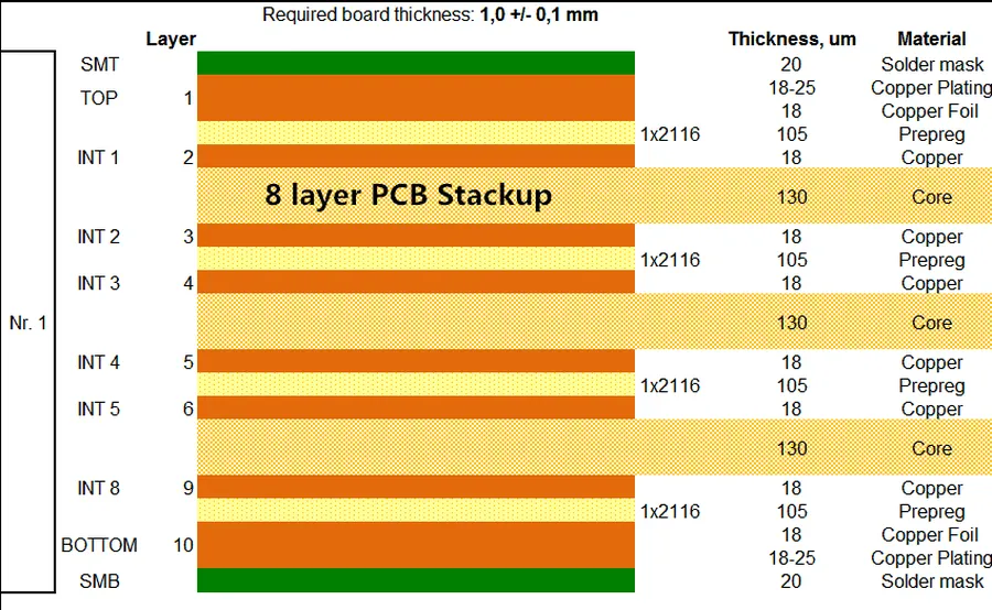
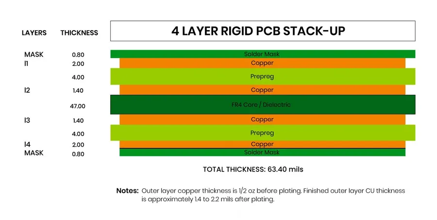
The stackup design of an 8-layer PCB is paramount for achieving optimal performance, influencing impedance control, signal integrity, and thermal management. A well-engineered stackup ensures that signal transmission is efficient, minimizing signal loss and crosstalk, while effectively managing heat dissipation. The arrangement of conductive layers and dielectric materials directly affects these critical parameters.
A skilled manufacturer plays a critical role, not only in executing the fabrication process but in advising on the optimal stackup configuration to ensure signal integrity and reliability. Understanding material properties, layer spacing, and the target application of the PCB are all essential to selecting the correct stackup for any given design.
| Parameter | Impact | Consideration |
|---|---|---|
| Layer Arrangement | Impedance control, signal integrity, power distribution | Careful placement of signal and power layers |
| Dielectric Material | Signal loss, thermal properties, cost | Selection of appropriate FR4, high-Tg, or other materials |
| Layer Thickness | Impedance, manufacturing feasibility | Trade-off between impedance requirements and practical etching limitations |
| Copper Weight | Current carrying capacity, heat dissipation | Matching copper weight to power requirements |
| Ground Planes | Signal return paths, noise reduction | Continuous ground planes for stable return paths |
Common stackup configurations often include dedicated ground and power planes, which significantly reduce noise and provide low impedance paths, improving signal integrity. For instance, a four-signal-layer stackup with embedded power and ground planes provides a balanced approach for both signal routing and power distribution. The key to effective stackup design is a thorough understanding of the intended application and specific performance requirements of the circuit.
Considerations such as controlled impedance for high-speed signals, material selection based on thermal needs, and the number of vias required for layer transitions are critical. A manufacturer with expertise in these parameters will be able to guide a design through the process from concept through to fabrication.
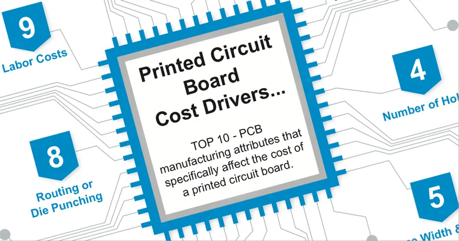
The cost of producing 8-layer PCBs is influenced by a multitude of factors, extending beyond just material costs. These drivers include design complexity, production volume, material selection, surface finish requirements, manufacturer location, lead times and desired precision, all of which contribute to the overall expense.
| Cost Factor | Description | Impact on Cost |
|---|---|---|
| Material Costs | Type of substrate (e.g., FR-4, High-Tg), copper thickness, and prepreg materials. | Higher cost for specialized materials (e.g., high-Tg, specific laminates). Increased copper thickness also raises cost. |
| Design Complexity | Number of vias, trace width and spacing, layer alignment accuracy, impedance control requirements. | Higher complexity leads to increased manufacturing difficulty, longer production times and potentially lower yields increasing cost. |
| Production Volume | Quantity of boards being manufactured in a single production run. | Higher volumes generally result in lower per-unit cost due to economies of scale. Small production runs are more expensive. |
| Surface Finish | Type of finish applied to the PCB (e.g., HASL, ENIG, Immersion Tin). | Premium finishes like ENIG increase cost compared to basic HASL due to the materials and processes required. |
| Manufacturer Location | Geographical location of the PCB manufacturer. | Manufacturers in some regions may offer lower labor costs or reduced overhead, which leads to lower prices. Other locations may have higher production costs. |
| Lead Times | Time required for the manufacturer to complete the PCB production. | Faster lead times often incur premium charges, whereas longer lead times may reduce production costs. |
| Desired Precision | Manufacturing tolerances, high precision requirements. | Tighter tolerances and higher precision require more advanced manufacturing processes, and may affect yield rates thus incurring additional costs. |
This section addresses common queries regarding 8-layer PCB manufacturing, providing clear and concise answers to help you navigate this complex topic. We aim to clarify key aspects, assisting you in making informed decisions when selecting a manufacturer.
The landscape of 8-layer PCB technology is rapidly evolving, driven by the increasing demands for higher performance, greater miniaturization, and enhanced reliability in modern electronics. These advancements are crucial for supporting emerging applications in high-speed data communications, artificial intelligence, and advanced medical devices, which require robust and efficient circuit boards.
Effective collaboration with your 8-layer PCB manufacturer is paramount to achieving high-quality, on-time, and within-budget production. This section provides actionable strategies for enhancing communication, ensuring file accuracy, and implementing quality control checkpoints throughout the development process.
Choosing the right 8 layer PCB manufacturer is pivotal for ensuring the quality, reliability, and performance of your electronic devices. Much like a bridge needs careful design and construction, the success of your advanced electronics project relies on a solid partnership with an expert manufacturer. From JLCPCB's rapid prototyping to PCBTok's advanced technologies, several options cater to specific needs and budgets. Consider stackup design, material selection, and lead time, and leverage the tips provided to foster a smooth collaboration process. By understanding your needs, asking the right questions and partnering with a qualified 8 layer PCB manufacturer, you can transform your vision into a tangible and successful product.

