In today's rapidly advancing technological landscape, the demand for sophisticated and reliable electronic systems is ever-increasing. High voltage applications, in particular, require precision engineering and unwavering stability to ensure both performance and safety. At Zero One Solution Limited, we understand these critical requirements. As a leading PCB solution provider specializing in rapid prototyping and one-stop services from design to assembly, we are at the forefront of delivering cutting-edge High Voltage Tester PCB Solutions. This article delves into the intricacies of these solutions, highlighting how our expertise empowers innovation and accelerates product development for industries where high voltage integrity is paramount.
Understanding High Voltage Tester PCB Solutions
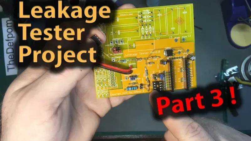
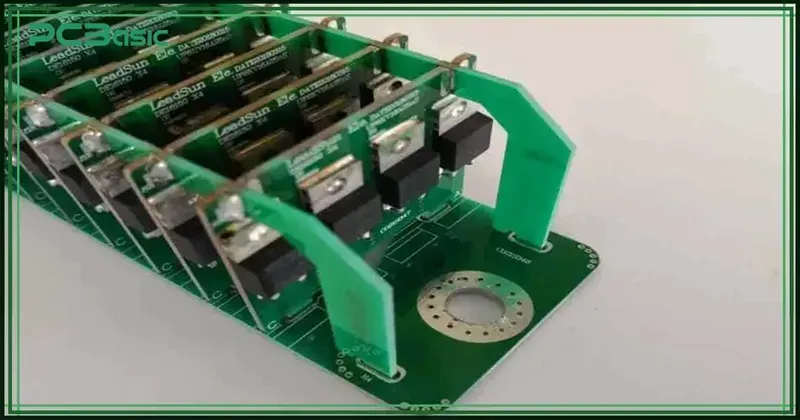
High Voltage Tester PCB Board
High Voltage Tester PCB Solutions are the critical backbone of systems designed to operate and test at elevated electrical potentials, ensuring safety, reliability, and precision across diverse high-power applications. These specialized Printed Circuit Boards (PCBs) are engineered to withstand significant electrical stress, isolate sensitive components, and facilitate accurate measurement and control within environments ranging from power electronics and industrial control systems to advanced medical devices. Their unique design and manufacturing considerations are paramount to mitigating risks like dielectric breakdown and ensuring long-term operational integrity.
What defines a "high voltage" PCB? While there's no single universal definition, a high voltage PCB typically involves operating voltages above 500V AC or 750V DC, where specialized design rules for creepage, clearance, and insulation are critical to prevent arcing, tracking, and breakdown. The specific threshold often depends on industry standards and application requirements, such as those set by IEC or UL for specific equipment types.
The importance of robust High Voltage Tester PCB Solutions spans multiple sectors, underpinning the performance and safety of essential equipment. In power electronics, they are integral to the efficiency and reliability of inverters, converters, and power supplies. For industrial control systems, they ensure the safe operation of heavy machinery and automation processes. In the medical field, their precision is vital for diagnostic imaging and therapeutic devices, where patient safety and accurate functionality are non-negotiable. Designing and manufacturing these PCBs presents inherent challenges, including managing extreme thermal loads, ensuring adequate isolation, and selecting materials that can withstand high dielectric stress over extended periods.
Key Design Considerations for High Voltage PCBs
Designing Printed Circuit Boards (PCBs) for high voltage applications presents unique challenges that demand meticulous attention to specific parameters. Unlike standard PCBs, High Voltage Tester PCBs operate under extreme electrical stress, necessitating advanced design strategies to prevent electrical breakdown, ensure operational safety, and guarantee long-term reliability. The cornerstone of successful high voltage PCB design lies in rigorously controlling creepage and clearance distances, selecting appropriate insulation materials, implementing robust thermal management, and carefully choosing components that can withstand high voltage environments.
Creepage and Clearance Distances Creepage is the shortest path between two conductive parts along the surface of the insulating material, while clearance is the shortest distance through the air between two conductive parts. For high voltage PCBs, these distances are paramount. Insufficient separation can lead to arc flashes and dielectric breakdown. Industry standards like IPC-2221 and IEC 60664-1 provide guidelines for minimum creepage and clearance based on voltage levels, pollution degree, and material group. Designers must often exceed these minimums, especially in critical applications, to build in safety margins and account for environmental factors such as humidity and dust.
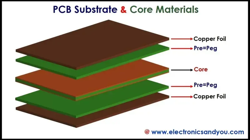
Insulation Materials and Dielectric Strength The choice of PCB substrate and prepreg materials directly impacts the board's ability to withstand high voltages. Materials must possess high dielectric strength, indicating their resistance to electrical breakdown. Common materials like FR-4 are often insufficient for very high voltage applications, necessitating alternatives such as Polytetrafluoroethylene (PTFE) or specific ceramic-filled laminates. Beyond the substrate, the selection of solder mask and conformal coatings is crucial, as these also contribute to insulation and protect against environmental degradation, increasing the effective creepage path.
Design Consideration
Impact on High Voltage PCB
Mitigation Strategy
Creepage Distance
Risk of surface arcing and tracking
Increase spacing, add slots or grooves, apply conformal coating
Thermal Management Strategies High voltage operation often generates significant heat due to power dissipation in components and traces. Excessive heat can degrade insulating materials, reduce component lifespan, and lead to thermal runaway. Effective thermal management involves designing for efficient heat dissipation. This includes using thicker copper layers for better heat spreading, incorporating thermal vias, strategically placing heat-generating components, and utilizing external heat sinks or active cooling solutions when necessary. Simulating thermal performance during the design phase is critical to identify and address hot spots before manufacturing.
By meticulously addressing these design considerations, Zero One Solution Limited ensures that our High Voltage Tester PCBs are not only robust and reliable but also comply with stringent safety and performance standards, enabling our clients to confidently develop and deploy advanced high-voltage systems.
Material Selection for Optimal High Voltage Performance
PCB Substrate Materials
Selecting the appropriate PCB substrate material is paramount for ensuring the long-term reliability, safety, and optimal performance of high voltage tester PCBs. The dielectric properties, thermal management capabilities, and environmental resilience of the chosen laminate directly impact the board's ability to withstand extreme electrical stresses without breakdown. At Zero One Solution Limited, our material selection process is meticulously designed to meet the rigorous demands of high voltage applications, mitigating risks and extending operational lifespans.
Material Type
Dielectric Strength (V/mil)
Thermal Conductivity (W/mK)
Moisture Absorption (%)
Typical High Voltage Application
FR-4 (Standard)
~1000
~0.25
0.10-0.20
General purpose, lower voltage
High Tg FR-4
~1000-1200
~0.25-0.30
0.05-0.15
Power supplies, industrial control
Polyimide (PI)
~3000-4000
~0.30-0.40
0.08-0.12
Aerospace, medical devices, flexible high voltage
PTFE (Teflon)
~1800-2000
~0.25
<0.01
RF/Microwave, high frequency high voltage
Ceramic (Alumina)
>5000
~20-30
<0.01
High power modules, extreme temperature
Dielectric Strength: This critical property determines a material's ability to withstand an electric field without breaking down. For high voltage PCBs, materials with superior dielectric strength are essential to prevent arc tracking and insulation failure.
Thermal Conductivity: High voltage applications often generate significant heat. Materials with good thermal conductivity are preferred to dissipate heat effectively, preventing hotspots that can degrade performance and lead to premature failure.
Moisture Absorption: Moisture can severely degrade a PCB's insulation properties, especially in high voltage environments. Low moisture absorption rates are crucial to maintain dielectric integrity and prevent electrical leakage.
Comparative Tracking Index (CTI): CTI measures a material's resistance to electrical breakdown and tracking on its surface. Higher CTI values indicate better resistance to carbonized paths forming under electrical stress, which is vital for long-term safety and performance in high voltage circuits.
Zero One Solution Limited leverages its extensive experience and global supply chain network to source and utilize only the highest-grade laminates. Our material engineers meticulously evaluate properties such as dielectric breakdown voltage, volume and surface resistivity, dissipation factor, and thermal expansion coefficients. This rigorous selection process ensures that every high voltage tester PCB we produce not only meets but often exceeds industry standards, delivering unparalleled safety and performance for our clients' most demanding applications.
Advanced Manufacturing Techniques for High Voltage Tester PCBs
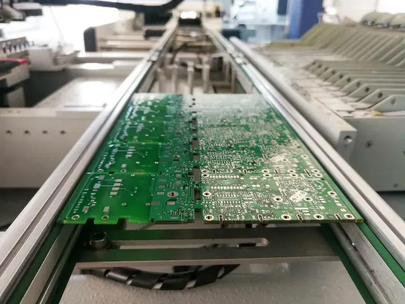
PCB Manufacturing Production Line
Manufacturing High Voltage Tester PCBs demands precision and specialized techniques to ensure long-term reliability and safety. Unlike standard PCBs, these boards require meticulous attention to detail in every step, from material preparation to final surface finish, to withstand extreme electrical stresses without breakdown. Zero One Solution Limited employs advanced manufacturing processes and state-of-the-art facilities to precisely control critical parameters, guaranteeing the integrity and performance of every high-voltage board produced.
Precise Etching and Imaging Achieving the precise trace widths and spacing necessary for high voltage isolation requires ultra-fine line etching capabilities. Our advanced imaging systems and chemical etching processes minimize undercut and ensure consistent geometry, critical for maintaining adequate creepage and clearance distances and preventing arc tracking.
Specialized Plating Processes The selection and application of plating materials are vital. We utilize specialized plating techniques, including immersion gold over electroless nickel (ENIG) or electroless palladium over immersion gold (EPIG), to provide robust, oxidation-resistant, and highly reliable surface finishes. These processes ensure excellent solderability and long-term connection integrity under high electrical loads, enhancing the overall durability of the High Voltage Tester PCBs.
Manufacturing Stage
Zero One Solution Limited's Advanced Approach
Benefit for High Voltage PCBs
Drilling & Via Formation
Controlled Depth Drilling, Laser Drilling
Minimizes delamination, ensures precise via integrity for high voltage paths, reduces partial discharge risk
Layer Alignment & Lamination
Automated Optical Alignment, Vacuum Lamination
Eliminates air voids and misalignments, crucial for preventing dielectric breakdown and enhancing insulation
Solder Mask Application
Precision Spray Coating, UV Curing
Ensures uniform, void-free solder mask coverage, critical for insulation and environmental protection
Surface Finishing
ENIG/EPIG, Selective Plating
Provides superior oxidation resistance, solderability, and withstands harsh operating conditions
Automated Optical Inspection (AOI)
High-Resolution AOI, X-ray Inspection
Detects microscopic defects, short circuits, open circuits, and misalignments invisible to the human eye, ensuring high reliability
Zero One Solution Limited's commitment to advanced manufacturing techniques is reinforced by stringent quality control measures at every stage. From incoming material inspection to in-process checks and final outgoing quality audits, our integrated quality management system ensures that every High Voltage Tester PCB meets the highest industry standards for performance, safety, and reliability. Our facilities, equipped with cutting-edge machinery and operated by experienced engineers, are designed to handle the complexities unique to high voltage applications, delivering unparalleled product quality.
Rigorous Testing and Quality Assurance for High Voltage Solutions
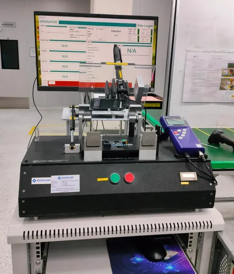
PCB Testing Equipment
For High Voltage Tester PCB Solutions, rigorous testing and unyielding quality assurance are not merely a final step, but the bedrock of reliability and safety. Given the critical nature of high voltage applications, any compromise in the PCB's integrity can lead to catastrophic failures, equipment damage, or even endanger lives. At Zero One Solution Limited, our comprehensive testing protocols go beyond industry minimums, employing advanced techniques like Hipot testing, insulation resistance validation, and thermal cycling to meticulously assess and confirm every PCB's ability to perform flawlessly under extreme electrical stress and varying environmental conditions, thereby ensuring unwavering compliance with the most stringent industry standards.
Hipot Testing (Dielectric Withstand Voltage Test) Hipot testing is paramount for high voltage PCBs. It involves applying a high voltage, significantly greater than the operational voltage, between conductors and ground to detect insulation breakdowns, inadequate creepage/clearance distances, or manufacturing defects that could lead to arcing or short circuits. This non-destructive test ensures the dielectric strength of the insulation material, confirming the PCB's ability to withstand voltage surges and prevent electrical breakdown, a critical safety measure in high voltage applications.
Insulation Resistance Testing This test measures the electrical resistance of the insulation material between conductors and ground. A high insulation resistance indicates good insulation properties, while a low reading can signal contamination, moisture ingress, or material degradation. Maintaining high insulation resistance is vital for preventing leakage currents, which can lead to energy loss, component degradation, and potential safety hazards over the PCB's operational lifetime, particularly in humid or harsh environments.
Thermal Cycling and Shock Testing High voltage PCBs often operate in environments with significant temperature fluctuations. Thermal cycling subjects the PCB to rapid changes in temperature, simulating real-world operational stress, to identify weaknesses in solder joints, material delamination, or component integrity. Thermal shock testing, an even more aggressive variant, evaluates the PCB's resistance to extreme and sudden temperature shifts, ensuring its mechanical and electrical stability across a wide temperature range, crucial for long-term reliability in demanding applications.
Automated Optical Inspection (AOI) and X-ray Inspection While not exclusively high voltage tests, AOI and X-ray inspection are integral to quality assurance. AOI systems use cameras to scan the PCB for surface defects, missing components, incorrect polarity, and solder joint quality. X-ray inspection provides a non-destructive view inside multi-layer PCBs and component packages, identifying hidden defects like voids in solder joints, misalignments, or internal short circuits, ensuring the foundational integrity of the board before high voltage testing.
Functional Testing and Performance Validation Beyond electrical and environmental stress tests, functional testing verifies that the High Voltage Tester PCB operates as designed under actual or simulated high voltage conditions. This includes validating output voltages, current handling capabilities, response times, and overall system performance. This final validation step confirms that the PCB meets all specified performance parameters and is ready for integration into the final high voltage testing equipment, guaranteeing optimal functionality and safety.
Zero One Solution Limited's Expertise in High Voltage PCB Solutions
Engineer Operating PCB
Zero One Solution Limited stands at the forefront of providing comprehensive High Voltage Tester PCB Solutions, leveraging over a decade of specialized experience to empower innovators in critical industries. Our expertise is rooted in a deep understanding of the unique challenges high voltage applications present, enabling us to deliver robust, reliable, and high-performance PCBs that meet stringent safety and operational standards. We are committed to accelerating your product development cycle through our distinctive rapid prototyping capabilities and a seamless one-stop service model.
Rapid Prototyping Excellence Our core strength lies in rapid-response R&D prototype manufacturing. We understand that time-to-market is critical for high-voltage innovations, and our agile processes ensure quick turnaround times without compromising on quality or reliability. This capability allows engineers to iterate designs swiftly, bringing their cutting-edge solutions to fruition faster and more efficiently than competitors. Our state-of-the-art facilities and experienced team are optimized for precision and speed, delivering functional prototypes that withstand rigorous high-voltage testing from the outset. Leveraging advanced machinery and refined workflows, we significantly reduce lead times for complex high-voltage PCB prototypes, enabling rapid validation and design optimization for our clients. We consistently achieve quick delivery of fully functional high-voltage prototypes, supporting diverse applications from power electronics to medical diagnostics and industrial control systems. This efficiency is critical for our clients' competitive advantage, allowing them to lead their respective markets with innovative products.
Our integrated approach streamlines the entire PCB development lifecycle, from initial design concepts to final manufacturing and assembly. This end-to-end service eliminates the complexities of coordinating multiple vendors, ensuring consistent quality, cost-effectiveness, and efficient project management. Zero One Solution Limited's comprehensive offerings include:
PCB Design and Layout for High Voltage Specialized design services incorporating critical high-voltage considerations such as creepage, clearance, insulation, and thermal management to ensure optimal performance and safety. Our design engineers utilize advanced simulation tools to predict and mitigate potential issues early in the design phase, ensuring compliance with industry standards like IPC-2221B and UL.
Service Aspect
Zero One Solution Limited Advantage
Client Benefit
Rapid Prototyping
Expedited R&D cycles (typically 3-7 days for complex HV PCBs)
Faster time-to-market, reduced development costs, quick design iteration
One-Stop Service
Integrated design, manufacturing, and assembly under one roof
Strategic locations in Shenzhen and Dubai, access to worldwide resources
Optimized material sourcing, enhanced resource availability, resilient supply chain against disruptions
Quality Assurance
Rigorous Hipot, insulation resistance, and thermal cycling tests
Guaranteed reliability, compliance with international safety standards, long-term operational stability
Our strategic locations in Shenzhen, China's electronic manufacturing hub, and a branch office in Dubai, position us uniquely within a robust global PCBA supply chain network. This dual presence ensures seamless access to premium raw materials, cutting-edge components, and a diverse talent pool, enabling us to manage projects efficiently and mitigate supply chain risks. We pride ourselves on delivering solutions that are not only technologically advanced but also globally accessible and cost-effective, solidifying our reputation as a trusted partner in the high-voltage electronics industry.
Case Studies: Successful High Voltage Tester PCB Implementations
High Voltage PCB Application Case
At Zero One Solution Limited, our commitment to excellence in High Voltage Tester PCB Solutions is best exemplified through the tangible successes of our clients. These case studies underscore our capability in transforming complex high-voltage requirements into reliable, high-performance PCB solutions, showcasing our expertise from rapid prototyping to final assembly. Each project highlights our meticulous approach to design, material selection, manufacturing, and rigorous testing, ensuring that our solutions meet and exceed the stringent demands of high-voltage applications across various industries.
Advanced Medical Imaging Device A leading medical technology company sought a High Voltage Tester PCB for their next-generation MRI scanner. The challenge involved integrating high-density components with extreme voltage isolation requirements while maintaining signal integrity. Zero One Solution Limited engineered a custom multi-layer PCB utilizing advanced FR-4 materials with enhanced dielectric properties and optimized creepage/clearance paths. Our rapid prototyping capabilities enabled quick iterations, leading to a final product that passed rigorous IEC 60601-1 compliance tests, significantly reducing development time and accelerating market entry for our client. The solution delivered exceptional stability and precision in high-voltage pulse generation, crucial for diagnostic accuracy.
Industrial Power Supply Unit for Renewable Energy For a major player in the renewable energy sector, we developed a High Voltage Tester PCB for a critical component within their solar inverter systems. The primary requirement was robust performance under fluctuating high voltages (up to 1500V DC) and harsh environmental conditions. We implemented a specialized laminate with superior thermal management properties and employed stringent manufacturing controls to ensure copper trace integrity and insulation resistance. Our comprehensive testing, including accelerated life testing and thermal cycling, validated the PCB's long-term reliability and efficiency. This project resulted in a 15% improvement in power conversion efficiency for our client's inverters, directly impacting energy yield and system longevity.
These case studies are a testament to Zero One Solution Limited's unwavering dedication to providing superior High Voltage Tester PCB Solutions. Our proven track record of successful implementations empowers our clients to innovate with confidence, knowing their high-voltage applications are built on a foundation of precision, reliability, and advanced engineering.
FAQs About High Voltage Tester PCB Solutions
Navigating the complexities of high voltage applications requires deep expertise in PCB design, manufacturing, and testing. To clarify common inquiries and address critical considerations for High Voltage Tester PCB Solutions, this section provides concise, expert answers to frequently asked questions, empowering you with the knowledge to make informed decisions for your high voltage projects.
What defines a "high voltage" PCB in the context of tester solutions? A "high voltage" PCB for tester solutions is typically defined by operating voltages exceeding 100V, often reaching kilovolts (kV). The critical factor isn't just the absolute voltage, but how it interacts with the PCB's material properties, trace spacing (creepage and clearance), and component insulation. These boards are designed to withstand significant electrical stress without breakdown, ensuring safety and performance in applications like power supplies, medical imaging, and industrial control systems where precise, high-voltage testing is paramount.
Why are creepage and clearance distances so crucial in High Voltage Tester PCB design? Creepage and clearance distances are paramount to preventing electrical breakdown and ensuring safety. Creepage is the shortest distance along the surface of an insulating material between two conductive parts, protecting against tracking. Clearance is the shortest distance through air between two conductive parts, preventing arc-over. In High Voltage Tester PCBs, inadequate spacing can lead to flashover, arcing, or material degradation over time, compromising tester accuracy, safety, and longevity. Strict adherence to IPC-2221/2221B standards and application-specific requirements is critical for reliable high voltage performance.
What specialized materials are essential for High Voltage Tester PCB Solutions? Specialized materials are crucial for High Voltage Tester PCB Solutions to withstand electrical stress and thermal demands. Key materials include substrates with high dielectric strength (e.g., polyimide, PTFE, or specific FR-4 variants with higher Comparative Tracking Index - CTI), low moisture absorption rates, and excellent thermal conductivity. For insulation, high-voltage-rated soldermasks and conformal coatings are often applied to enhance surface insulation resistance and mitigate environmental effects. These material choices directly impact the PCB's long-term reliability and safety under high voltage conditions.
How does Zero One Solution Limited ensure the reliability of High Voltage Tester PCBs? Zero One Solution Limited ensures the reliability of High Voltage Tester PCBs through a multi-faceted approach. This includes rigorous adherence to industry standards (e.g., IPC), precise design rule checking for creepage and clearance, selection of high-performance dielectric materials, and advanced manufacturing processes like controlled impedance etching and specialized plating. Post-manufacturing, comprehensive testing protocols such as Hipot (dielectric withstand voltage) testing, insulation resistance testing, and thermal cycling are performed to validate board integrity, ensuring every PCB meets the stringent performance and safety requirements for high voltage applications.
What is the typical lead time for rapid prototyping of High Voltage Tester PCB Solutions? The typical lead time for rapid prototyping of High Voltage Tester PCB Solutions at Zero One Solution Limited varies based on design complexity, material availability, and order volume. However, our specialized rapid prototyping capabilities are designed to significantly accelerate this process. For standard high-voltage designs, prototypes can often be delivered within 5-10 business days. For highly complex or specialized material requirements, the timeline may extend slightly, but we consistently strive to optimize efficiency and minimize turnaround times to help clients accelerate their product development cycles.
In conclusion, developing and implementing robust High Voltage Tester PCB Solutions is a complex but crucial endeavor for ensuring the safety, reliability, and performance of electronic systems in demanding environments. At Zero One Solution Limited, our comprehensive expertise, rapid prototyping capabilities, and commitment to quality position us as your ideal partner in navigating these challenges. From initial concept and precise PCB design to advanced manufacturing and assembly, we provide a seamless, one-stop service that significantly accelerates your time to market. Partner with Zero One Solution Limited to transform your high voltage testing requirements into reliable, high-performance realities. Contact us today to discuss your next project and experience the Zero One Solution Limited difference.