
In the race for ultra-fast mobile charging, the Printed Circuit Board Assembly (PCBA) is the beating heart of every premium power bank. Selecting the wrong component leads to thermal runaway, protocol failures, and dissatisfied customers. As modern devices demand higher wattages, engineers must balance compact form factors with robust energy management. This guide breaks down the mission-critical factors required to specify high-performance PCBA solutions that stand up to real-world stress.
Understanding Power Protocol Compatibility
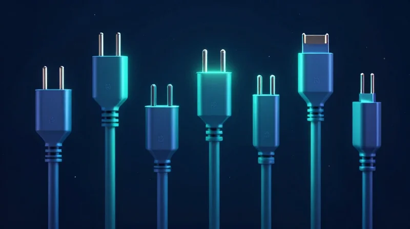
The Landscape of Fast Charging Standards
Selecting the right PCBA requires navigating a fragmented ecosystem where industry-standard protocols coexist with manufacturer-specific fast-charging technologies. For premium portable power banks, compatibility is not merely a feature—it is the primary determinant of perceived device quality and user satisfaction.
| Protocol Type | Primary Application | Key Advantage |
|---|---|---|
| USB-PD (Power Delivery) | Universal Laptops/Smartphones | High power output (up to 240W) |
| Qualcomm QC (Quick Charge) | Legacy Android Devices | Wide install base and maturity |
| Proprietary (VOOC/SCP/FCP) | Brand-specific Flagships | Optimized thermals and speed |
Critical Compatibility Considerations
A high-performance PCBA must negotiate power delivery dynamically. When the power bank fails to communicate correctly with the sink device, charging defaults to basic 5V/1A or 5V/2A speeds, leading to poor user experiences. Engineers must prioritize support for Programmable Power Supply (PPS) within the USB-PD specification, as it allows for fine-grained voltage adjustments that minimize heat dissipation during charging cycles.
Frequently Asked Questions
- Why is USB-PD 3.0 PPS support mandatory for premium designs?
PPS allows the power bank to adjust its output voltage in real-time increments, which is critical for maintaining compatibility with modern smartphone super-charging requirements and improving thermal efficiency. - Does supporting multiple protocols increase PCBA cost significantly?
While multi-protocol support increases bill-of-materials (BOM) complexity due to the need for advanced controller ICs, it drastically improves the market versatility of the power bank, often justifying the investment through higher product positioning. - How does proprietary protocol support affect backward compatibility?
Premium PCBAs use intelligent protocol handshake chips that prioritize standard USB-PD but fall back to secondary protocols, ensuring that devices from brands like Samsung, Xiaomi, or Huawei still receive optimized charging speeds.
Thermal Management Strategies for High Wattage
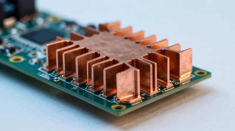
Substrate Material and Copper Weight Optimization
To handle currents exceeding 5A in modern fast-charging portable power banks, the PCBA substrate must exhibit high thermal conductivity and excellent glass transition temperatures (Tg). Standard FR-4 is often insufficient for sustained high-wattage outputs; therefore, high-Tg materials (above 170°C) are recommended to maintain structural integrity under continuous load. Furthermore, increasing copper weight—typically moving from standard 1oz to 2oz or 3oz foils—drastically reduces ohmic resistance, which minimizes heat generation directly at the source.
Thermal Dissipation Techniques
Beyond material selection, heat must be efficiently transported away from critical components like MOSFETs and buck-boost controllers. Strategic implementation of thermal vias and integrated heat spreaders is essential.
| Strategy | Mechanism | Primary Benefit |
|---|---|---|
| Thermal Vias | Copper-filled vias connecting component pads to internal ground planes. | Distributes heat away from localized hotspots. |
| Heat Spreaders | Copper cladding or metal plates attached via TIM. | Increases effective surface area for passive cooling. |
| Active Throttling | Firmware-based power scaling via NTC thermistors. | Prevents hardware damage during extreme ambient conditions. |
Thermal Management FAQ
- Why is copper weight critical for fast charging?
Higher copper weight lowers the track resistance (DCR), which reduces I²R power losses that would otherwise convert into excess heat during high-current delivery. - When should active thermal throttling be triggered?
Throttling should be calibrated based on the NTC thermistor readings at the MOSFET junction; typically, a soft-clamping of output power is triggered at 85°C to prevent a hard shutdown. - Does PCB layout affect thermal performance?
Yes, proper component placement—keeping high-current power stages away from sensitive control logic—is vital to prevent cross-heating and ensure accurate sensor readings.
Evaluating Component Reliability and Sourcing
Critical Component Selection for Longevity
The operational lifespan of a fast-charging PCBA is primarily dictated by the quality of its passive and active components. In high-power designs where current densities are significant, utilizing sub-par capacitors or MOSFETs can lead to rapid degradation, increased ESR (Equivalent Series Resistance), and eventual thermal runaway.
| Component Category | Key Reliability Metric | Recommended Standard |
|---|---|---|
| Capacitors | ESR & Ripple Current | Automotive-grade or Industrial Solid Polymer |
| MOSFETs | RDS(on) & Thermal Margin | Low RDS(on) Trench/SGT Technology |
| Inductors | Saturation Current | Shielded Metal Composite |
Sourcing Strategies and Quality Assurance
To prevent premature module failure, manufacturers must prioritize authorized distribution channels to mitigate the risks associated with counterfeit or refurbished components. Implementing a robust Bill of Materials (BOM) auditing process is critical for premium product tiers.
- How do I verify component authenticity?
Always source through franchised distributors. Cross-reference batch codes with manufacturers' traceability documentation to ensure silicon provenance. - Why are automotive-grade components preferred?
Automotive-grade components undergo more rigorous stress testing for vibration, thermal cycling, and humidity compared to standard commercial components, providing superior reliability. - How does component degradation impact safety?
Degradation in capacitors or protection ICs often leads to inaccuracies in voltage sensing, which can trigger over-voltage protection failures or overheating during high-wattage cycles.
Efficiency Metrics and Conversion Losses

Quantifying Conversion Efficiency
Efficiency in a fast-charging PCBA is defined as the ratio of output power delivered to the device versus the power drawn from the internal battery cells. In high-power applications, even a small percentage drop in efficiency translates into significant waste heat, which accelerates component degradation and reduces the effective mAh rating available to the end-user.
| Efficiency Level | Thermal Impact | Usable Capacity Impact |
|---|---|---|
| Below 85% | High (Requires active cooling) | Substantial loss (~15%+) |
| 85% - 92% | Moderate (Standard passive) | Optimal performance |
| Above 92% | Minimal (Advanced GaN design) | Maximum capacity delivery |
Common Sources of Conversion Loss
- Switching Losses in MOSFETs
Occurs during the rapid on-off switching states of the power stage; selecting high-frequency GaN FETs significantly reduces these losses compared to traditional Silicon MOSFETs. - Inductor DCR Losses
Resistance in the inductor windings leads to energy dissipation as heat; using low-DCR (Direct Current Resistance) components is vital for high-wattage charging. - PCB Trace Impedance
Poorly optimized trace routing or insufficient copper weight creates voltage drops that force the regulator to work harder, lowering overall system efficiency.
Strategies to Minimize Energy Waste
To select a PCBA that maximizes power delivery, focus on the synchronous rectification architecture and the switching frequency control loop. Synchronous rectification, which replaces diodes with controlled MOSFETs, is essential for reducing conduction losses at high currents. Furthermore, designers should look for PCBAs that utilize adaptive frequency scaling, which adjusts the switching frequency based on load conditions, maintaining peak efficiency across a wide range of output voltages from 5V to 20V.
Safety Protections: OVP, OCP, and OTP
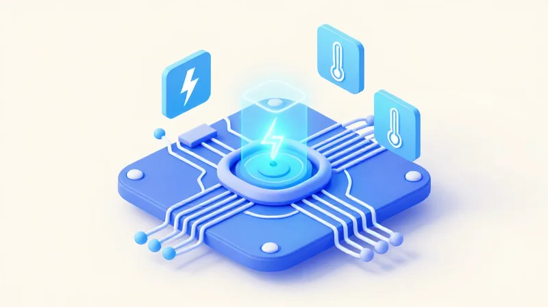
Essential Safety Protections for High-Power Charging
In the context of high-wattage power delivery, the PCBA must act as an intelligent gateway that monitors electrical and thermal states in real-time. Without robust hardware-level safeguards, high-current delivery risks catastrophic battery failure or damage to sensitive mobile device chipsets. Designers must prioritize ICs that feature cycle-by-cycle monitoring to ensure these protections remain responsive under varying load conditions.
| Feature | Primary Function | Failure Risk Mitigation |
|---|---|---|
| OVP (Over-Voltage) | Detects input/output surges | Prevents voltage spikes from damaging the target device or battery cells. |
| OCP (Over-Current) | Monitors current thresholds | Stops runaway current draw that could lead to PCB trace melting or fire. |
| OTP (Over-Temperature) | Tracks junction/cell heat | Initiates thermal throttling or emergency shutdown to prevent thermal runaway. |
Technical Implementation FAQs
- How does hardware-based OCP differ from software-based limits?
Hardware-based OCP utilizes comparator circuits that act near-instantaneously to cut the power path, whereas software limits depend on MCU sampling rates, which may be too slow to prevent damage during a direct short circuit. - Where should NTC thermistors be placed for optimal OTP?
For maximum effectiveness, NTC thermistors should be placed in direct physical contact with the battery pack and adjacent to the primary power-switching MOSFETs, as these are the two main heat-generating points. - What is the importance of Hysteresis in protection circuits?
Hysteresis prevents 'chattering' or rapid oscillation between on and off states once a threshold is reached, ensuring the PCBA stays in a safe state until the underlying fault is fully cleared.
When sourcing, always verify that the chosen power delivery controller IC includes these features at the silicon level rather than relying on external discrete components. Integrated protections significantly reduce the PCBA footprint and decrease the response time during critical faults, which is essential for maintaining certification standards like UL or IEC 62368-1.
Physical Form Factor and Integration Constraints
The integration of high-power fast charging circuitry into a premium portable power bank is a delicate exercise in spatial optimization. As power densities rise, the PCBA must handle significant thermal loads within a shrinking physical footprint. Successful integration depends on a synergistic relationship between board layout, chassis airflow, and the strategic positioning of heat-generating components.
Managing Component Density and Thermal Loads
When selecting a PCBA, prioritize modules that utilize advanced packaging, such as GaN-based power stages, which reduce the required surface area for equivalent power conversion. Board density is limited by the thermals of the inductor and FET array. Always evaluate the board's thermal interface material (TIM) mounting points, as high-power boards must be physically coupled to the chassis to dissipate heat effectively.
| Feature | Integration Impact | Optimization Strategy |
|---|---|---|
| Connector Orientation | Affects Z-height | Use low-profile SMT USB-C ports |
| Inductor Height | Limits case thickness | Select low-profile shielded inductors |
| Thermal Coupling | Prevents thermal throttling | Ensure board features landing pads for thermal pads |
Common Integration Constraints FAQ
- How does connector placement impact chassis structural integrity?
Improper alignment of USB-C or Lightning connectors can exert mechanical stress on the PCBA solder joints during user insertion. Ensure the PCBA design features robust metal reinforcement or chassis-mounted bracket support for all I/O ports. - Why is board Z-height critical for slim designs?
Premium power banks target sub-15mm thicknesses. Selecting a PCBA with tall electrolytic capacitors or bulky through-hole inductors often mandates a thicker, less aesthetically pleasing chassis design. - Can I use double-sided PCBAs in thin power banks?
Yes, but double-sided populated boards require careful attention to chassis clearance. Ensure no components interfere with battery cells, and use Kapton tape or isolation sheets to prevent accidental shorts if clearances are less than 0.5mm.
Finally, verify that your selected PCBA includes standardized mounting hole patterns that align with your enclosure's standoffs. Misaligned mounting points introduce physical torque that can fracture brittle ceramic capacitors or solder fillets over time, leading to premature field failure.
Testing Protocols for Quality Assurance
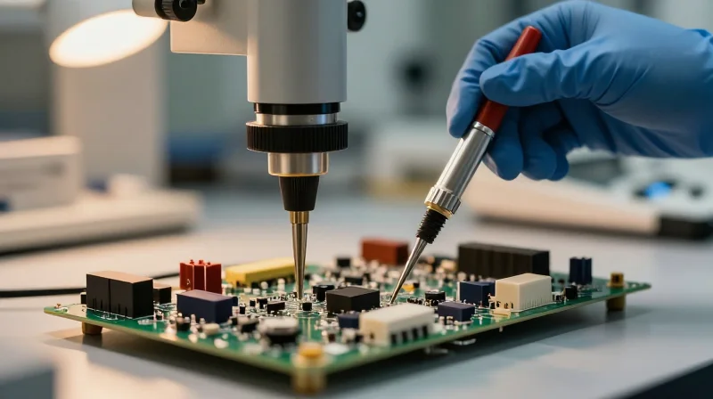
Validation of Peak Load Performance
To guarantee that a PCBA can sustain advertised wattage without failure, engineers must subject the hardware to comprehensive stress testing under peak load conditions. This involves operating the board at maximum output capacity in a temperature-controlled environment to monitor component stability and thermal degradation over extended periods.
| Test Type | Objective | Key Metric |
|---|---|---|
| Thermal Stress Test | Verify heatsink and component thermal limits | Maximum Junction Temperature |
| Full Load Endurance | Ensure consistent power output over 48+ hours | Output Ripple Voltage |
| Transient Response | Evaluate recovery from sudden load changes | Voltage Overshoot/Undershoot |
Critical Safety Compliance Testing
Beyond standard performance, the PCBA must undergo fault-injection testing to ensure that protection circuitry triggers correctly during catastrophic events or user error.
- How do we test Over-Voltage Protection (OVP)?
Manually introduce voltage spikes above the rated threshold to verify the controller disconnects the load within milliseconds. - Is short-circuit testing mandatory?
Yes; the PCBA must demonstrate the ability to enter a latch-off or hiccup mode immediately when output pins are shorted without physical component rupture. - How is Over-Temperature Protection (OTP) validated?
Apply external heat or simulate high current draw until the thermistors report reaching critical thresholds, confirming the system throttles or shuts down gracefully.
Best Practices for Reliable Quality Assurance
To achieve consistent yield rates, manufacturers should integrate automated optical inspection (AOI) during the PCBA assembly process. Following assembly, functional testing (FCT) should be performed on every unit to calibrate output current limiters and verify firmware integrity before the final enclosure assembly.
Future-Proofing Your Power Bank Design
The Role of GaN in Future-Proofing
Gallium Nitride (GaN) is no longer a luxury; it is the baseline for premium portable power. By replacing traditional Silicon-based MOSFETs with GaN-on-Si components, designers can significantly increase power density while reducing thermal dissipation. Future-proofing your PCBA requires selecting controllers that are natively compatible with GaN's high switching frequencies, allowing your product to remain relevant as output wattage requirements continue to climb.
Adaptability to Evolving Charging Protocols
Market standards such as USB Power Delivery (PD) 3.1 are pushing limits beyond 140W. A design trapped in a legacy protocol will quickly become obsolete. To maintain a competitive edge, utilize programmable PD controllers that support firmware updates via a USB interface, allowing for protocol patches even after the units are deployed to the field.
| Feature | Legacy Approach | Future-Proof Strategy |
|---|---|---|
| Switching Material | Silicon MOSFETs | GaN-on-Si Technology |
| Protocol Support | Fixed Hardware ICs | Firmware-Upgradable PD Controllers |
| Thermal Management | Heatsink-heavy | High-efficiency topology (LLC/Active Clamp) |
Frequently Asked Questions
- How does USB PD 3.1 impact my current PCBA design?
USB PD 3.1 introduces Extended Power Range (EPR) up to 48V/5A. If your current PCBA is limited to 20V/5A, it will be incompatible with next-generation high-performance laptops and workstations. - Is modularity necessary for a premium power bank?
Yes. Decoupling the charging logic from the power stage allows you to upgrade the primary controller when new standards arrive without requiring a complete redesign of the mechanical chassis. - Will GaN components become more cost-effective?
As supply chains scale, the price gap between GaN and Silicon is closing rapidly. Investing in GaN today avoids the sunk cost of redesigning your PCB to meet thermal efficiency requirements tomorrow.
Selecting the optimal PCBA is not merely a component choice; it is a design commitment to safety and efficiency. By focusing on thermal dynamics and protocol flexibility, you ensure your portable power bank remains a top-tier product in a competitive market. Ready to elevate your hardware design? Contact our engineering team today for expert consultation on custom PCBA sourcing solutions.
