In today's world, where we spend a significant portion of our lives indoors, monitoring and maintaining indoor environmental quality is paramount. From homes and offices to hospitals and schools, the air we breathe and the conditions we experience within these spaces directly impact our health, comfort, and productivity. As a leading PCB solution provider, Zero One Solution Limited recognizes the critical need for accurate and reliable indoor environment monitoring. This article delves into our specialized PCB solutions designed to empower effective and efficient indoor environment monitoring, providing insights into the technology, applications, and benefits of these solutions. We'll explore how these PCB solutions contribute to creating healthier, more comfortable, and more productive indoor environments.
Indoor environment monitoring, facilitated by advanced PCB solutions, is fundamentally critical for safeguarding human health, enhancing comfort, and optimizing productivity across various settings. With individuals spending an estimated 90% of their time indoors, as per the U.S. Environmental Protection Agency (EPA), the quality of the indoor environment directly impacts well-being and operational efficiency. Precise monitoring of factors like air quality (PM2.5, VOCs, CO2), temperature, and humidity, enabled by robust PCB design, allows for proactive adjustments to HVAC systems and ventilation, mitigating health risks associated with pollutants and ensuring optimal conditions for occupants and sensitive equipment.
| Environmental Factor | Impact of Poor Monitoring | Benefit of Effective Monitoring |
|---|---|---|
| Air Quality (PM2.5, VOCs, CO2) | Increased respiratory issues, reduced cognitive function, stale air syndrome | Improved health, enhanced alertness, fresh indoor environment |
| Temperature | Discomfort, decreased productivity, equipment malfunction | Optimized comfort, peak performance, stable equipment operation |
| Humidity | Mold growth, dust mites, static discharge, material degradation | Mold prevention, reduced allergens, equipment longevity |
| Lighting | Eye strain, circadian rhythm disruption, low morale | Enhanced visual comfort, improved mood, increased productivity |
| Noise Levels | Distraction, stress, hearing impairment | Reduced stress, better concentration, quieter working/living spaces |
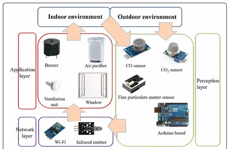
A robust Indoor Environment Monitoring (IEM) system hinges on the seamless integration of several core components, each playing a critical role in data collection, processing, and communication. Understanding these essential elements is fundamental to designing and implementing effective solutions that provide accurate, real-time insights into indoor conditions. From the precise capture of environmental parameters to the intelligent interpretation and secure transmission of data, each module contributes to a comprehensive and reliable monitoring infrastructure.
| Component Category | Key Components | Primary Function | Zero One Solution's PCB Contribution |
|---|---|---|---|
| Sensing Layer | Temperature & Humidity Sensors (e.g., DHT11, BME280) | Detect and convert physical environmental parameters into electrical signals. | High-precision analog and mixed-signal PCB layouts for accurate sensor integration and minimal noise interference. Optimized thermal management zones. |
| Component Category | Key Components | Primary Function | Zero One Solution's PCB Contribution |
|---|---|---|---|
| Sensing Layer | Particulate Matter Sensors (e.g., PMS5003, SDS011) | Measure concentrations of airborne particulates (PM2.5, PM10). | Dedicated power isolation and optimized signal paths to prevent interference from sensor heating elements; compact design for tight spaces. |
| Component Category | Key Components | Primary Function | Zero One Solution's PCB Contribution |
|---|---|---|---|
| Sensing Layer | Volatile Organic Compound (VOC) Sensors (e.g., SGP30, MQ-series) | Detect harmful gaseous pollutants and assess overall air quality. | Specialized layouts to ensure sensor stability and responsiveness, often requiring specific material considerations for chemical resistance. |
| Component Category | Key Components | Primary Function | Zero One Solution's PCB Contribution |
|---|---|---|---|
| Sensing Layer | Carbon Dioxide (CO2) Sensors (e.g., MH-Z19, SCD30) | Monitor CO2 levels for ventilation assessment and occupant comfort. | Precise power delivery and signal integrity for NDIR (Non-Dispersive Infrared) sensors, often accommodating larger sensor footprints. |
| Component Category | Key Components | Primary Function | Zero One Solution's PCB Contribution |
|---|---|---|---|
| Data Acquisition & Processing | Microcontrollers (MCUs) / Microprocessors (MPUs) (e.g., ESP32, STM32) | Collect, process, and analyze raw sensor data; manage system operations. | Complex multi-layer PCB designs supporting high-speed digital signals, power efficiency, and integration of various peripheral interfaces (I2C, SPI, UART). |
| Component Category | Key Components | Primary Function | Zero One Solution's PCB Contribution |
|---|---|---|---|
| Communication Module | Wi-Fi, Bluetooth, LoRa, Cellular (e.g., ESP8266, SIM800) | Transmit processed data to cloud platforms or local displays. | RF-optimized PCB layouts with impedance control and proper antenna matching for reliable and efficient wireless communication; support for various wireless standards. |
| Component Category | Key Components | Primary Function | Zero One Solution's PCB Contribution |
|---|---|---|---|
| Power Management | Voltage Regulators, Battery Management ICs | Ensure stable and efficient power supply to all components. | Robust power planes, efficient heat dissipation, and optimized component placement for thermal stability and extended battery life in portable applications. |
Zero One Solution Limited excels in designing and manufacturing PCBs that form the backbone of these sophisticated monitoring systems. Our rapid prototyping capabilities and deep understanding of sensor integration ensure that the printed circuit boards are not merely carriers but active enablers of precise data collection and reliable operation, even in challenging indoor environments. We leverage advanced materials and manufacturing techniques to minimize signal noise, optimize power consumption, and ensure long-term stability and accuracy for all integrated components.
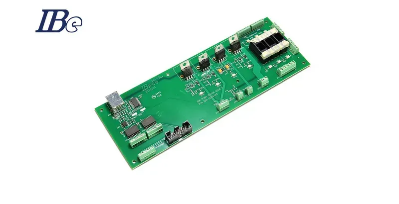
Zero One Solution Limited stands at the forefront of providing bespoke PCB solutions optimized for the stringent demands of indoor environment monitoring. Leveraging over a decade of specialized experience in rapid prototyping and high-precision manufacturing, we offer comprehensive, one-stop services from initial PCB design to final assembly. Our solutions are engineered to ensure unparalleled accuracy, reliability, and longevity for a diverse range of environmental sensing applications, establishing us as a critical partner in developing advanced monitoring systems.
| Feature | Zero One Solution Limited's Advantage | Benefit to Environmental Monitoring Systems |
|---|---|---|
| Rapid Prototyping | Expedited turnaround on initial designs and revisions | Accelerates product development cycles and time-to-market for innovative monitoring devices |
| Design for Manufacturability (DFM) | Early-stage identification and resolution of potential manufacturing issues | Reduces production costs and improves overall product reliability and yield |
| Global Supply Chain Network | Strategic access to diverse components and materials worldwide | Ensures consistent material availability and competitive pricing, enhancing project scalability |
| Post-Production Support | Comprehensive technical assistance and troubleshooting | Guarantees long-term operational stability and performance of monitoring solutions |
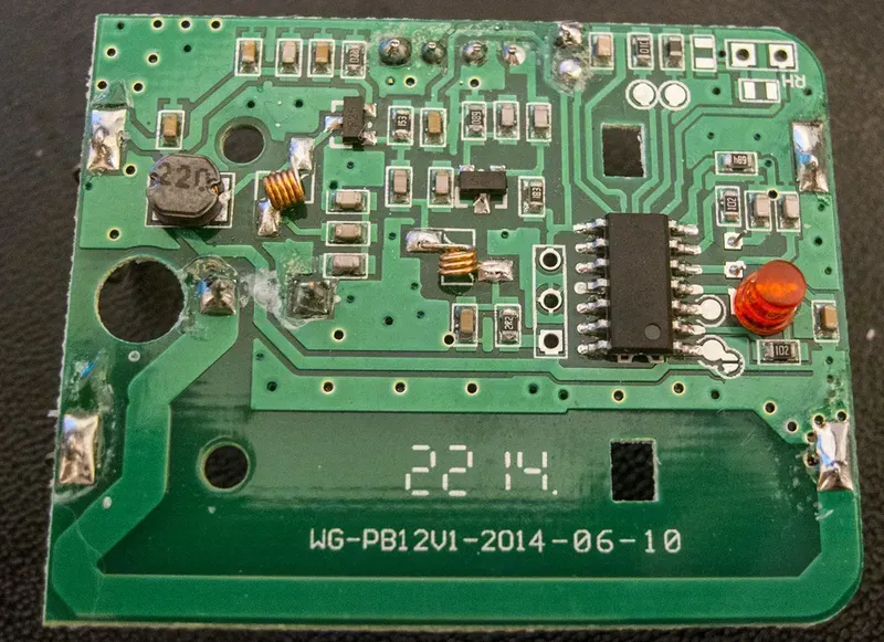
Achieving highly accurate and reliable sensor readings in Indoor Environment Monitoring (IEM) systems hinges critically on meticulous PCB design. Beyond merely connecting components, the printed circuit board acts as the foundational platform, directly influencing signal integrity, thermal dissipation, and overall system longevity. Thoughtful consideration of factors like sensor placement, signal routing, noise reduction, and thermal management during the design phase is paramount to ensuring that environmental data collected is both precise and actionable, preventing erroneous interpretations that could lead to suboptimal environmental control or even health concerns.
| Design Consideration | Impact on Sensor Performance | Best Practices for IEM PCBs |
|---|---|---|
| Sensor Placement | Directly affects measurement accuracy due to localized environmental variations or proximity to heat/EM sources. | Strategically place sensors away from heat-generating components (e.g., microcontrollers, power regulators). Consider airflow and typical measurement points within the monitored space. |
| Signal Routing | Improper routing can introduce noise, crosstalk, and signal degradation, especially for analog sensor signals. | Employ differential routing for sensitive analog signals, keep traces short and direct, and maintain proper impedance matching. Isolate analog and digital grounds if necessary. |
| Noise Reduction | Electrical noise (EMI/RFI) can corrupt sensor readings, leading to inaccurate data. | Implement proper grounding techniques (star grounding, ground planes), use shielding, integrate decoupling capacitors close to ICs, and consider common-mode chokes on power lines. |
| Thermal Management | Temperature fluctuations or hotspots on the PCB can affect sensor calibration and operational accuracy, particularly for temperature and humidity sensors. | Utilize copper pours for heat dissipation, strategically place thermal vias, consider heat sinks for high-power components, and ensure sufficient board area for heat spreading. Validate thermal performance with simulation. |
| Component Selection | Quality and characteristics of passive and active components can significantly impact sensor signal integrity and stability. | Select low-noise operational amplifiers, high-precision resistors, and stable capacitors. Choose components with appropriate temperature coefficients for the operating environment. |
| Material Selection | PCB substrate material properties affect signal loss, impedance stability, and environmental resilience. | Opt for standard FR-4 for most applications. For high-frequency or extreme environments, consider specialized laminates with stable dielectric constants and low dissipation factors. Ensure material compatibility with sensor type (e.g., low outgassing for VOC sensors). |
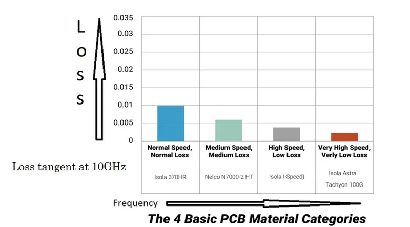
The foundation of a reliable Indoor Environment Monitoring PCB Solution lies in the meticulous selection of materials. This critical choice directly impacts the sensor's accuracy, long-term stability, and overall system performance, especially in diverse environmental conditions. Opting for materials with appropriate dielectric properties, low moisture absorption, and excellent thermal stability is paramount to prevent signal degradation and ensure precise data acquisition for critical indoor environmental parameters.
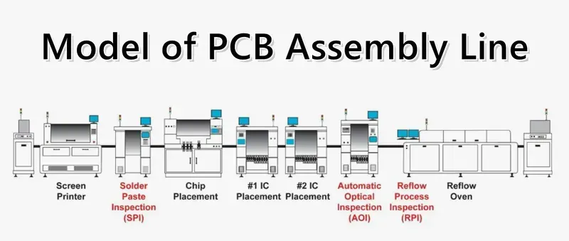
Zero One Solution Limited stands at the forefront of PCB manufacturing and assembly, offering specialized expertise crucial for the demanding requirements of Indoor Environment Monitoring (IEM) systems. Our advanced capabilities ensure that every PCB functions optimally, from precision component placement to robust soldering techniques, all underpinned by rigorous quality control. This meticulous approach directly translates into the reliability and accuracy essential for critical environmental data collection.
| Aspect of Expertise | Zero One Solution Limited's Approach | Impact on IEM PCBs |
|---|---|---|
| Precision Component Placement | Automated pick-and-place machines with micron-level accuracy for even the smallest passive and active components. | Ensures proper electrical connections and sensor functionality, critical for accurate environmental data acquisition. |
| Advanced Soldering Techniques | Utilizing reflow, wave, and selective soldering with optimized thermal profiles for diverse component types and materials. | Minimizes thermal stress, prevents cold joints, and enhances the longevity and reliability of sensor connections in varying indoor climates. |
| Automated Optical Inspection (AOI) | High-resolution optical systems inspect every solder joint and component for defects, misalignments, and polarity issues. | Detects subtle manufacturing flaws early, preventing costly failures and ensuring consistent sensor performance. |
| X-Ray Inspection (AXI) | Non-destructive inspection for hidden solder joints (e.g., BGA, QFN) and internal defects. | Verifies the integrity of complex component connections, crucial for robust data processing and communication modules within IEM systems. |
| Functional Testing (FCT) | Custom-designed test fixtures and sequences to verify the electrical and functional performance of the assembled PCB. | Confirms that all sensors, communication interfaces, and processing units operate as designed, ensuring system readiness for deployment. |
| Environmental Testing (Optional) | Accelerated life testing, temperature cycling, and humidity exposure to simulate real-world conditions. | Validates the long-term reliability and stability of the PCB under typical indoor environmental fluctuations, guaranteeing consistent performance. |
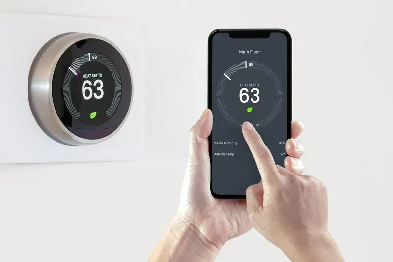
Indoor Environment Monitoring PCB Solutions are the foundational enablers of intelligent systems designed to create healthier, more comfortable, and energy-efficient indoor spaces. These specialized PCBs are meticulously engineered to integrate diverse sensors and communication modules, translating environmental data into actionable insights for a wide array of applications, from ensuring occupant well-being in homes and offices to optimizing operational efficiency in commercial and industrial settings. Their versatility makes them indispensable in the evolving landscape of smart buildings and IoT ecosystems.
Partnering with Zero One Solution Limited for your indoor environment monitoring PCB solutions provides a distinct competitive edge, combining rapid innovation with unwavering quality and supply chain resilience. Our deep-rooted expertise, honed over years in the PCB assembly solutions industry, ensures that your vision for precise and reliable environmental monitoring translates into high-performance, market-ready products with unparalleled efficiency.
Zero One Solution Limited has leveraged its 20 years of experience in PCB design and manufacturing to address the complexities of indoor environment monitoring systems. Our approach focuses on delivering optimal sensor performance and system reliability, ensuring our clients can develop cutting-edge solutions for smart buildings, HVAC, and industrial applications. Our commitment to excellence is reflected in our rigorous design and manufacturing processes, which include advanced simulation and testing to meet stringent environmental monitoring standards.
In conclusion, Zero One Solution Limited's Indoor Environment Monitoring PCB Solutions offer a comprehensive and reliable platform for creating healthier and more productive indoor spaces. By leveraging our expertise in PCB design, manufacturing, and assembly, we empower our clients to develop cutting-edge environmental monitoring devices that contribute to improved well-being. Whether you're developing air quality monitors, smart thermostats, or integrated building management systems, our PCB solutions provide the foundation for accurate, efficient, and reliable environmental sensing. Contact Zero One Solution Limited today to discuss your indoor environment monitoring PCB needs and discover how we can help you create innovative solutions for a healthier future. Let's work together to build a world where everyone can breathe easier and thrive in their indoor environments.

