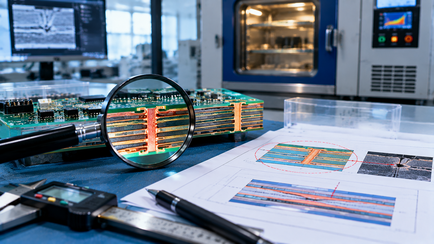
HDI PCB long-term failures are rarely caused by a single defect. They result from materials, lamination processes, copper distribution, dielectric thickness, moisture, contamination, and operating stress acting together.
Microvia cracking is often the focus, but it's not the only failure mode. Deeper mechanisms may pass standard qualification tests yet emerge after months or years of use.
During lamination, resin flows to fill gaps and bond layers. When resin is insufficient, resin starvation occurs — leaving voids, incomplete bonding, or insufficient encapsulation.
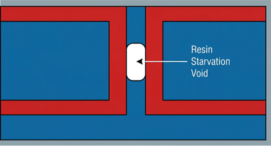
Why HDI is more susceptible:
Sequential lamination cycles consume available resin
High-density copper features require more fill
Fine-pitch structures create narrow gaps that resist resin flow
Consequences: Local delamination or moisture-absorbing voids that enable CAF growth and electrochemical migration.
Prevention: Balance copper density, match prepreg resin content to copper volume, optimize lamination, and use DFM tools to flag at-risk areas.
Each lamination cycle subjects copper and dielectric to thermal stress. Since they expand at different rates, interfacial adhesion must withstand shear stress.
Why HDI is more sensitive: In 3-N-3 HDI designs, the innermost core experiences four lamination cycles before assembly. Accumulated stress weakens adhesion, especially at feature edges.
Manifestations: Pad lifting, trace delamination, annular ring separation — these create stress concentration points that accelerate cracking.
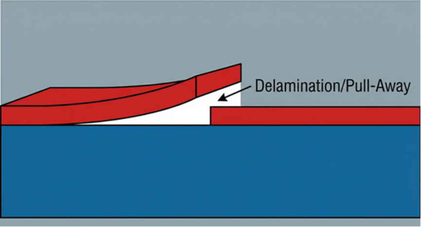
Prevention: Confirm the material system has been validated for the required lamination cycles. Copper surface treatment also affects bond durability.
HDI stackups use very thin dielectric layers (2–4 mil) to achieve target impedance and minimize thickness. These thin layers are more susceptible to mechanical deformation.
Causes: Press-fit connectors, heatsinks mounted with fasteners, non-uniform lamination pressure, and handling bending.
Prevention: Avoid thin dielectrics in high-stress areas, use stiffeners to distribute loads, and specify handling requirements to limit board bending.
Under bias voltage and moisture, conductive copper filaments grow along glass fiber interfaces. HDI's tight via spacing and thin dielectrics shorten the bridging distance. CAF may take months or years to cause a short circuit.
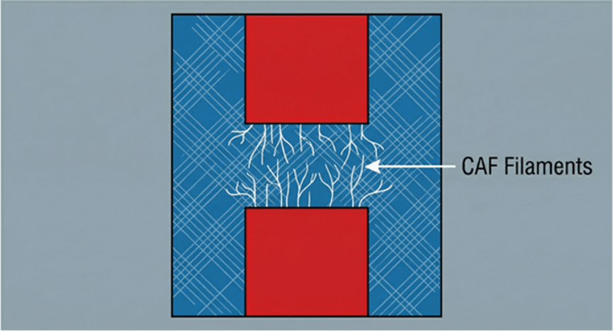
A marginal microvia may pass initial thermal cycling but slowly crack under operating stress, eventually causing intermittent or permanent failure.
Ionic contamination and moisture cause metal dendrites to grow between conductors under bias voltage. Flux residue, fingerprints, or environmental contamination provide the ionic species. Failure time depends on contamination level, moisture, and conductor spacing.
Via-in-pad places solder joints above filled microvias. If fill is not perfectly flat or has different CTE than surrounding copper, the joint experiences extra stress. This accelerates fatigue, especially in high-reliability applications.
| Measure | Description |
|---|---|
| Material Selection | Select materials validated for required lamination cycles; confirm CAF resistance rating matches conductor spacing and environment |
| Copper Balance | Balance copper density across the board to promote uniform resin flow and minimize warpage |
| DFM Analysis | Flag resin starvation risk, annular ring violations, and other HDI-specific issues before release |
| Extended Testing | For high-reliability applications, extend thermal cycling and incorporate moisture exposure |
| Cleanliness | Specify and verify ionic cleanliness levels appropriate for HDI geometry and environment |
HDI technology enables capabilities traditional methods cannot achieve. To realize them without sacrificing reliability, engineers must understand these failure mechanisms and proactively prevent them during design.
Key Takeaways:
Resin starvation: Sequential lamination consumes resin; balance copper density and match prepreg
Copper delamination: Multiple cycles accumulate stress; validate material for cycle count
Dielectric crush: Thin layers are stress-sensitive; distribute loads and specify handling
Latent failures: CAF, slow cracking, migration, and solder fatigue may appear after months or years
Prevention: Material validation, copper balance, DFM analysis, extended testing, cleanliness specs
Need HDI PCB Design and Manufacturing Support?
AnyPCBA supports 2-64 layers with HDI, rigid-flex, and high-frequency hybrid processes. Our engineering team provides DFM/DFA design reviews to help identify potential issues in stackup, copper balance, resin flow, and CAF risk.
Contact us to discuss your project →




