
Introduction: Pads are the basic building blocks of surface mount assembly. They form the land pattern of a PCB and serve both electrical connection and component fixation. This guide covers common pad types—square, round, island, polygonal, oval, and open—along with special pads like thermal relief, star, and teardrop pads, and the key design standards for pad shape, size, hole diameter, and reliability.
Description: Based on AnyPCBA's small-to-medium volume PCB and PCBA manufacturing experience, this guide explains PCB pad types and design standards—covering pad shape, size, hole diameter, reliability requirements, and how DFM review catches pad-related manufacturing risks before production.
In PCB design, the pad is a fundamental concept. PCB engineers are certainly familiar with it. But while familiar, many engineers only have partial knowledge of pads.
A pad is the basic building block of surface mount assembly. It forms the land pattern of a circuit board—the combination of pads designed for specific component types. Pads serve electrical connection, component fixation, or both.
This guide covers PCB pad types and the key design standards.
Square pads: Used when components on the board are large but few, and routing is simple. Easy to implement in hand-made PCBs.
Round pads: Widely used in single-sided and double-sided boards with regularly arranged components. If board density allows, pads can be larger to prevent detachment during soldering.
Island pads: Pads and their connecting traces merged into one. Commonly used in vertical, irregularly arranged installations.
Polygonal pads: Used to distinguish pads with similar outer diameters but different hole sizes, facilitating processing and assembly.
Oval pads: Provide enough area to enhance peel resistance. Commonly used for dual in-line packages.
Open pads: Used to ensure that pad holes for manual touch-up soldering are not sealed by solder after wave soldering.
Star (plum blossom) pads
Star pads are typically used at large grounded through-hole locations. There are two reasons for this design:
Mounting holes need to be metallized and connected to GND. If the hole is fully metallized, it can easily be blocked during reflow soldering.
Internal metal screw holes may develop poor grounding due to installation or repeated disassembly. With star pads, good grounding is maintained regardless of stress changes.
Thermal relief (cross) pads
Thermal relief pads, also called heat pads or hot air pads, reduce heat dissipation from the pad during soldering, preventing cold joints or PCB blistering caused by excessive heat loss.
When the pad is a ground connection, thermal relief reduces the connected ground area and slows heat dissipation, making soldering easier.
When the PCB requires machine placement and reflow soldering, thermal relief pads prevent PCB blistering (because more heat is needed to melt the solder paste).
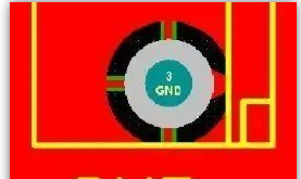
Thermal relief pad: the cross-shaped connections reduce heat dissipation during soldering, making it easier to reach soldering temperature.
Teardrop pads
Used when the trace connected to the pad is thin, to prevent pad peeling and trace-to-pad separation. Commonly used in high-frequency circuits.
Use standard PCB footprint libraries.
Minimum pad single-side dimension not less than 0.25mm; maximum pad diameter not more than 3 times the component hole diameter.
Ensure the spacing between two pad edges is greater than 0.4mm.
Pads with hole diameter exceeding 1.2mm or pad diameter exceeding 3.0mm should be designed as diamond or star pads.
In dense routing, oval and elongated pads are recommended. Single-sided board pad diameter or minimum width is 1.6mm; double-sided board weak-current pad only needs hole diameter plus 0.5mm. Pads that are too large can cause unnecessary solder bridging.
Pad inner holes are generally not smaller than 0.6mm, because holes smaller than 0.6mm are difficult to punch. Typically, the metal pin diameter plus 0.2mm is used as the pad inner hole diameter. For example, if a resistor's metal pin diameter is 0.5mm, its pad inner hole diameter is 0.7mm. Pad diameter depends on inner hole diameter.
Symmetry: To ensure balanced surface tension of molten solder, both ends of the pad must be symmetrical.
Pad spacing: Spacing that is too large or too small causes soldering defects. Ensure proper spacing between component ends or pins and pads.
Pad remaining dimension: The remaining dimension after component end or pin overlaps the pad must ensure the solder joint can form a meniscus.
Pad width: Should be basically consistent with the width of the component end or pin.
As a factory focused on small-to-medium volume PCB and PCBA manufacturing, AnyPCBA has accumulated years of experience in pad design. Our manufacturing capabilities cover 2 to 64 layers, including HDI, rigid-flex, and high-frequency hybrid. We hold ISO 13485 (medical) and IATF 16949 (automotive) certifications.
During DFM review, we focus on pad-related design issues:
Whether pad dimensions match component pins: pads that are too small result in insufficient solder strength; pads that are too large increase bridging risk. For small packages like 0201 and 0402, pad dimension precision requirements are higher.
Whether thermal relief design is reasonable: for pads connected to ground or power planes, evaluate whether thermal relief is needed. Thermal relief reduces heat dissipation and facilitates soldering, but improper design can affect electrical performance.
Whether teardrop pads are necessary: for thin trace connection points, teardrop pads prevent pad peeling and trace breakage. In high-density designs, however, teardrop pads consume extra space and require trade-offs.
Whether pad spacing meets process requirements: spacing that is too small causes bridging; too large causes insufficient solder strength. For fine-pitch components (such as 0.4mm pitch BGA), pad spacing design is especially critical.
Pad-to-solder-mask relationship: matching solder mask opening size to pad size directly affects soldering quality. Too small an opening covers the pad; too large allows solder to flow where it shouldn't.
Our engineers help you confirm these pad design details at the design stage, so your boards are not only drawable, but stable and reliable to produce.
If you're working on PCB design, or want to learn more about pad design issues, contact us through our website.
What pad design challenges have you encountered? Share your experience in the comments.




