Introduction: A PCB stack-up determines signal integrity, power integrity, EMI/EMC performance, and manufacturing cost. When designing boards with four or more layers, stack-up decisions directly impact board performance and price. This guide covers stack-up fundamentals, key design principles, and how stack-up choices affect circuit performance.
Description: Based on AnyPCBA's small-to-medium volume PCB manufacturing experience, this guide explains PCB stack-up design principles—from signal integrity and power integrity to manufacturing constraints—and how stack-up choices affect circuit performance, cost, and manufacturability.
In PCB design, the stack-up is the invisible skeleton that determines the board's performance, signal integrity, and manufacturing cost.
When designing simple single-sided or double-sided boards, there is usually no need to consider complex stack-up issues—you simply choose a copper-clad laminate that meets the required copper thickness and board thickness. But when designing a PCB with four or more layers, the stack-up design directly affects both performance and price.
This article explains the fundamentals of PCB stack-ups, the core design principles, and how stack-up choices affect circuit performance.
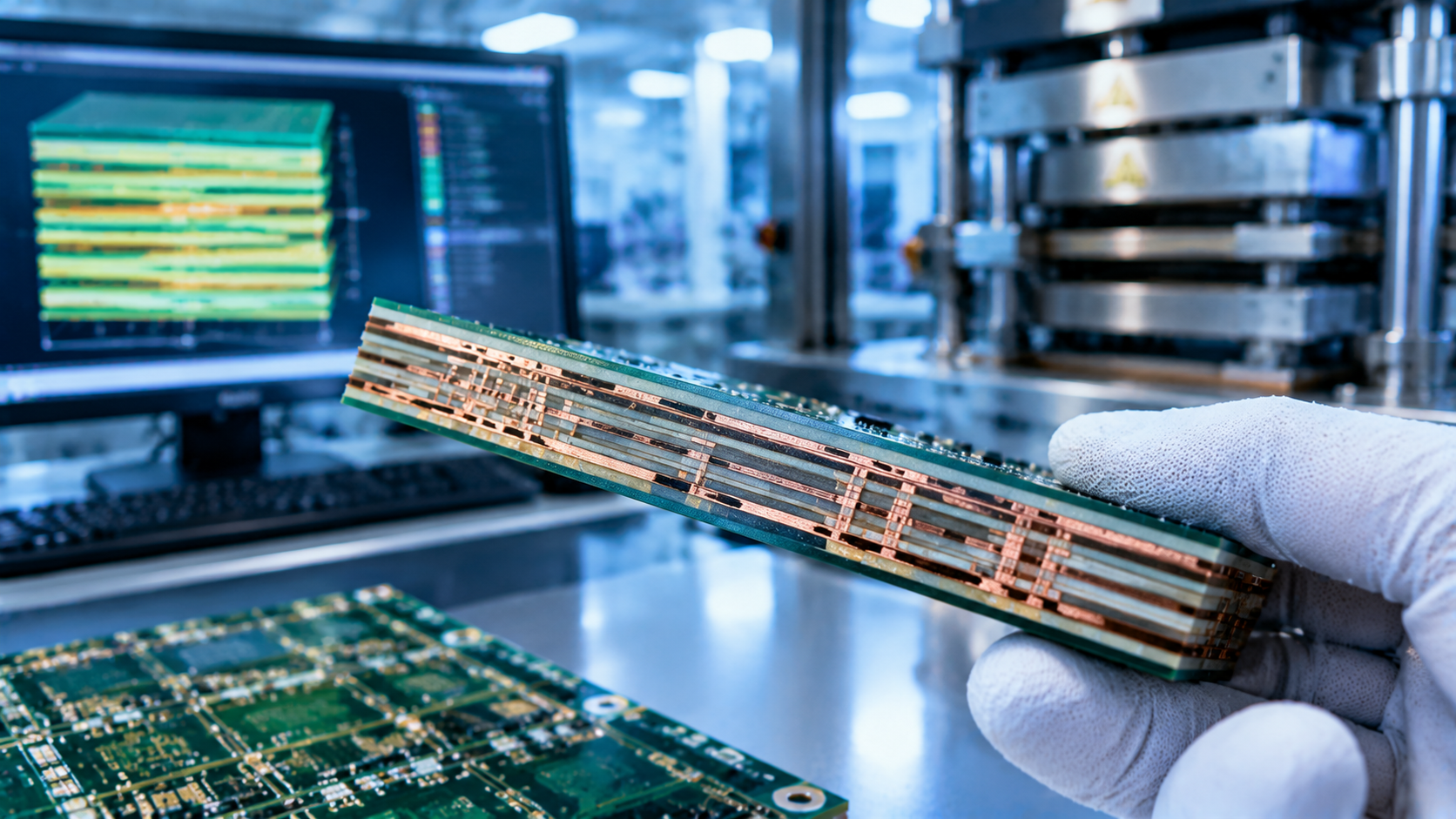
A multilayer PCB is built by combining copper-clad cores (Core), prepreg (PP), and copper foil according to the stack-up design, then pressing them together under heat and pressure.
Before PCB layout begins, the layout engineer determines the layer count based on board dimensions, circuit complexity, and electromagnetic compatibility (EMC) requirements. Then they determine component placement, and finally the division of signal, power, and ground layers.
Stack-up design requires comprehensive consideration of layer count, signal types, board thickness, material selection, copper thickness, impedance control, EMI/EMC shielding, thermal management, cost, and testability.
Build GND/Signal/GND combinations: For critical signal traces, the adjacent signal layers should be stripline, with ground planes above and below. This minimizes crosstalk coupling.
Microstrip vs. stripline: Use stripline (inner layers) for critical high-speed signals, and microstrip (surface layers) for non-critical high-speed signals.
Avoid broadside-coupled stripline: Unless absolutely necessary, avoid broadside-coupled stripline. Exposure and etching offsets during PCB manufacturing can cause misalignment, making fabrication difficult and impedance consistency hard to guarantee.
Adjacent signal and inner power layers: Each signal layer should be placed directly adjacent to an inner power or ground layer, and effectively isolated from other signal layers to reduce crosstalk.
Multiple reference ground planes: Consider using multiple reference ground planes to enhance electromagnetic absorption. For example, in a 10-layer board design, if there is only one power layer, an S G S S G P S S G S stack-up can be used. If two power layers are needed, consider S G S S G P S S P S.
In specific stack-up configurations, increasing the spacing between certain layers can control crosstalk. For example, increase the spacing between signal layer S1 and S2, or between S3 and S4.
Stack-up design is not just a structural diagram—it directly determines the physical characteristics of the circuit:
Improved power quality, reduced crosstalk and EMI: A well-planned stack-up (with signal layers adjacent to power or ground planes) optimizes electromagnetic field distribution and reduces coupling interference between layers.
Cost savings and higher integration: Within limited space, increasing layer count enables more functionality without increasing PCB area, meeting the miniaturization trend of modern electronics.
Enhanced noise immunity: Introducing insulation layers in the stack-up reduces circuit interference and ensures accurate high-speed, high-frequency signal transmission.
Reduced transmission delay: Short-distance transmission between layers significantly reduces signal propagation time, which is critical for high-speed data applications.
As a factory focused on small-to-medium volume PCB and PCBA manufacturing, AnyPCBA has accumulated years of experience in multilayer lamination and impedance control.
Our manufacturing capabilities cover 2 to 64 layers, supporting HDI, rigid-flex, high-frequency hybrid, and heavy copper boards. We hold ISO 13485 (medical) and IATF 16949 (automotive) certifications.
During DFM review, we focus on the following stack-up details to prevent production failures:
Stack-up symmetry: If copper thickness and dielectric thickness are not consistent top and bottom, warpage is highly likely after lamination, leading to SMT placement offset. AnyPCBA recommends symmetrical structures whenever possible.
Prepreg resin fill: If there are large copper areas (such as high-current power layers), evaluate whether the prepreg resin flow can completely fill the gaps to avoid delamination.
Impedance design manufacturability: Confirm whether the customer's specified trace width, spacing, and dielectric thickness are within the factory's etching tolerance. AnyPCBA performs TDR impedance testing before production.
Layer registration accuracy: For high-layer-count boards, layer registration is a challenge. We use high-precision alignment equipment to ensure via and trace alignment accuracy.
Stack-up design is about finding the balance between performance, cost, and manufacturing difficulty. Choosing the right stack-up and aligning with a manufacturer who understands fabrication is essential for high-speed, high-reliability PCBA design.
If you want to learn more about AnyPCBA's stack-up capabilities and impedance control process, or need our DFM team to review your current stack-up design, contact us through our website.