Introduction: PCB warpage and bowing are common defects during SMT reflow soldering, caused by thermal stress from mismatched CTE between copper, resin, and fiberglass. This article covers five key strategies to prevent warpage—lowering thermal stress, using high-Tg materials, increasing board thickness, optimizing board dimensions and panelization, and using reflow carriers—along with AnyPCBA's manufacturing control practices.
Description: Based on AnyPCBA's small-to-medium volume PCB and PCBA manufacturing experience, this guide explains how to prevent PCB warpage and bowing during reflow—from material selection and board thickness to panelization and reflow carriers—and how DFM review and process control keep thin and large boards flat.
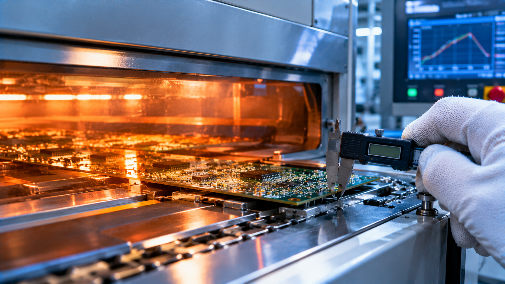
In SMT assembly, after the pick-and-place machine places all components, the PCBA must pass through the reflow oven. But under the high temperatures of reflow, PCBA boards are highly susceptible to bowing (Bow) and twisting (Twist).
Even slight deformation can cause component shift and cold joints. Severe deformation can crack BGA chips or prevent the board from fitting into the enclosure. How do we prevent warpage during reflow? This article covers five key strategies, combined with AnyPCBA's manufacturing experience in process control.
The root cause of warpage is thermal stress. A PCB is laminated from different materials—copper foil, resin, and fiberglass—each with different coefficients of thermal expansion (CTE). When the board passes through the high-temperature zone of the reflow oven (typically 240°C to 260°C), these materials expand at different rates. Combined with the board's own weight, the result is irreversible deformation after cooling.
Since temperature is the primary source of stress, lowering the peak reflow temperature or slowing the ramp-up and cooling rates can significantly reduce warpage.
Caution: This approach has side effects. If the temperature is lowered too much or ramped too slowly, solder may not fully melt (cold joints), or flux may not volatilize properly, causing short circuits or cold solder joints.
Tg (glass transition temperature) is the temperature at which a material transitions from a glassy state to a rubbery state.
Lower Tg materials soften faster upon entering the reflow oven and stay in the rubbery state longer, resulting in more severe deformation.
Higher Tg materials can better withstand stress deformation.
Trade-off: High-Tg laminates (Tg 170 or higher) cost more. But for automotive, industrial, and other high-reliability applications, this is a necessary cost.
Many electronic products reduce board thickness to 1.0mm, 0.8mm, or even 0.6mm for thin form factors. At such thicknesses, maintaining flatness through reflow is extremely difficult.
AnyPCBA recommendation: Unless extreme thinness is required, use a standard 1.6mm board thickness. This greatly reduces the risk of warpage.
Most reflow ovens use chains to transport boards.
Long-edge orientation: Larger boards sag under their own weight between the chains. Orient the long edge of the board along the chain direction to minimize sag.
Control panel count: More boards in a panel means a larger area and greater deformation. Orient the narrow edge perpendicular to the reflow direction for minimum sag.
If the above methods are difficult to implement, use a reflow carrier to reduce deformation.
Principle: The carrier holds the board rigid during both thermal expansion and contraction. Once the board cools below its Tg and re-hardens, it retains its original dimensions.
Double-sided carriers: If a single-layer carrier isn't enough, add a top cover to sandwich the board between two layers. This dramatically reduces warpage through reflow.
Trade-off: Carriers are expensive and require manual loading and unloading, reducing line efficiency.
As a factory focused on small-to-medium volume PCB and PCBA manufacturing, AnyPCBA has developed effective process controls for thin boards, large boards, and high-layer-count boards:
DFM-stage intervention: During design review, if we detect a board thinner than 1.0mm and large in size, we flag it early and recommend symmetrical stack-up design or adding breakaway rails to balance stress.
Custom reflow carriers: For PCBA prone to warpage, we build custom Durostone carriers. This material withstands high temperatures without deforming, effectively controlling PCBA deformation at high temperature.
Optimized reflow profiles: We create specific temperature profiles for different board thicknesses and sizes. While ensuring solder quality, we flatten ramp and cooling rates as much as possible to reduce thermal shock.
Real-time monitoring: On the line, we use a KIC profiler to monitor board surface temperature in real time, ensuring the actual profile matches the setpoint.
AnyPCBA focuses on small-to-medium volume PCB and PCBA manufacturing from 5 to 5,000 pieces, with extensive experience in medical electronics, industrial control, automotive electronics, and other high-reliability soldering applications. If you're designing thin or large boards and are concerned about reflow warpage, contact us through our website.