
In the fast-paced world of IoT, a brilliant product design can be rendered useless by poor assembly-ready execution. For engineers working with WiFi modules, the intersection of radio frequency performance and manufacturability is where projects either thrive or fail validation. This guide provides the technical roadmap to mastering DFM for WiFi-enabled boards, ensuring your hardware is as reliable in production as it is in the lab.
Understanding the DFM-Wireless Nexus

When transitioning from standard digital logic boards to WiFi-enabled hardware, the primary challenge is the management of high-frequency electromagnetic interference. Unlike static digital signals, WiFi radio frequency (RF) circuits are hyper-sensitive to manufacturing variations, including copper surface roughness, dielectric consistency, and component placement tolerances. Achieving success in small-batch manufacturing hinges on recognizing that the board is no longer just an interconnection medium, but an active component of the antenna system.
Comparative Analysis: Digital vs. RF-Integrated PCBAs
| Parameter | Standard Digital PCBA | WiFi-Enabled PCBA |
|---|---|---|
| Trace Impedance | Standard tolerance (±10%) | Precision controlled (±5%) |
| Component Placement | Dense packing permitted | RF-isolation distance required |
| Layer Stackup | Cost-optimized | Electromagnetically symmetrical |
| DFM Focus | Assembly yield | Signal integrity and EMI |
Key DFM Constraints for WiFi Modules
- Controlled Impedance Vias
Stubs left over from through-hole vias can act as antennas, causing unwanted resonance. Blind or buried vias are often required for high-frequency WiFi signal paths. - Ground Plane Integrity
Discontinuities in the ground plane beneath an RF trace cause impedance mismatch. The DFM process must ensure an unbroken return path directly beneath the signal line. - Component Proximity
Switching power supplies and digital clocks must be physically shielded or isolated from the wireless module to prevent noise coupling into the sensitive RF frontend.
Failing to account for these variables during the design phase often leads to failed FCC/CE testing or degraded range, both of which are costly to remediate in small-batch production. By integrating RF-DFM principles early, manufacturers can minimize the iteration cycles required for radio certification.
Critical Antenna Placement and Grounding Strategy
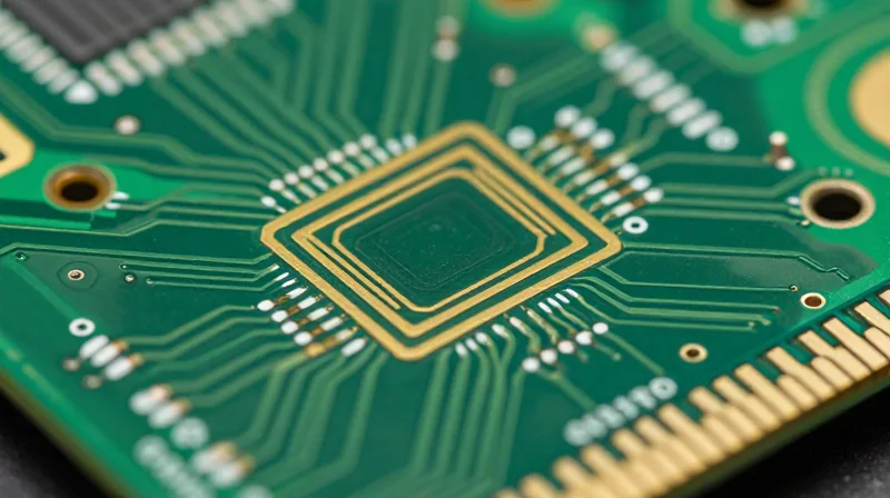
Critical Antenna Placement and Grounding Strategy
Achieving signal integrity in WiFi-enabled PCBA requires a synergistic approach to antenna positioning and ground plane design. The primary goal is to minimize parasitic capacitance and ensure consistent impedance while mitigating electromagnetic interference (EMI) generated by high-speed digital lines.
Antenna Placement and Clearance Zones
The antenna is the most sensitive component of your design. Implementing a 'keep-out' area is mandatory to prevent detuning and signal blockage. Ideally, the antenna should be placed at the board edge, overhanging the main chassis if necessary to maintain a clear line-of-sight.
| Design Factor | Best Practice | Reasoning |
|---|---|---|
| Component Proximity | Maintain >15mm distance | Prevents near-field coupling |
| Copper Pours | Clearance zone below antenna | Eliminates parasitic capacitance |
| Metal Chassis | Use non-conductive enclosures | Prevents signal attenuation |
Ground Plane Integrity
For WiFi modules, the ground plane acts as the return path for the antenna's RF signal. Splitting ground planes or introducing large cutouts can create massive impedance mismatches. Maintain a solid, low-impedance ground plane directly beneath the module while enforcing strict 'keep-out' zones beneath the trace leading to the antenna.
- How do I handle vias near the RF trace?
Avoid stitching vias directly under the transmission line. Use ground copper pours on adjacent layers and ensure they are connected to the main ground at intervals smaller than 1/10th of the wavelength. - Is a partial ground plane acceptable?
No. A partial ground plane creates return currents that follow longer paths, increasing loop area and EMI. Always prioritize a continuous reference plane for RF traces. - How does PCB thickness affect the RF path?
Dielectric thickness directly influences the trace width required for 50-ohm impedance matching. Always verify the stackup with your manufacturer before routing the RF line.
Advanced Trace Routing for High-Frequency Signals

Advanced Trace Routing for High-Frequency Signals
At WiFi frequencies (2.4 GHz and 5/6 GHz), copper traces cease to function as simple interconnects and instead behave as transmission lines. To achieve signal integrity, you must maintain a consistent 50-ohm characteristic impedance by meticulously calculating trace geometry based on your specific PCB stack-up and dielectric constants.
Microstrip vs. Stripline Considerations
| Feature | Microstrip | Stripline |
|---|---|---|
| Routing Layer | Outer Layers | Internal Layers |
| EMI Performance | Moderate (Requires shielding) | Superior (Self-shielding) |
| Trace Speed | Faster (Lower dielectric) | Slower (Higher propagation delay) |
| Manufacturing | Easier impedance control | Requires balanced stack-up |
Mitigating EMI with Via Stitching
Via stitching acts as a 'Faraday cage' for high-frequency traces. When routing sensitive RF signals, place ground vias along the sides of the transmission line, spaced at no more than 1/10th of the signal's effective wavelength. This effectively ties reference planes together, preventing the formation of resonant slots and reducing radiative EMI.
- How do I calculate precise trace width?
Utilize industry-standard solvers like Saturn PCB Toolkit or Polar Si9000, inputting your target impedance, dielectric constant (Dk), and distance to the reference plane. - Why should I avoid 90-degree trace bends?
Sharp corners create local increases in trace width, resulting in impedance discontinuities and reflections that degrade WiFi SNR; use 45-degree or rounded arcs instead. - What is the impact of stubs?
Unterminated trace segments (stubs) act as antennas at high frequencies. Always prune stubs near via transitions to prevent signal distortion.
Mitigating Interference with Component Placement
Strategic Isolation of RF and Digital Domains
Effective interference mitigation in small-batch WiFi PCBA hinges on strict spatial partitioning. High-speed switching components, such as DC-DC converters and high-frequency clock oscillators, generate significant broadband noise that can easily couple into sensitive WiFi RF front-ends. To maintain signal integrity, designers must enforce a 'zoning' approach where the RF circuit block is physically separated from high-noise digital switching regulators by a minimum of 10-15mm or by a dedicated ground-shielding trench.
Comparing Noise Suppression Strategies
| Interference Source | Primary Mitigation | Implementation Detail |
|---|---|---|
| DC-DC Switching Noise | Decoupling/Filtering | Place inductors away from RF traces and add ferrite beads. |
| Digital Crosstalk | Spatial Isolation | Enforce keep-out zones between high-speed logic and RF paths. |
| Power Supply Ripple | Point-of-Load Regulation | Use dedicated LDOs for the WiFi chipset power rails. |
Mitigating Power Supply Noise
WiFi chipsets are notoriously sensitive to power supply ripple. If switching noise from a local regulator couples onto the WiFi voltage rail, it will manifest as phase noise, degrading the EVM (Error Vector Magnitude) and limiting the effective range of the device. Designers should employ a multi-stage filtering approach, utilizing low-ESR ceramic capacitors placed as close as possible to the module's VDD pins and utilizing a dedicated LDO to isolate the RF power path from the primary system power.
Common Implementation Questions
- Can I place high-speed digital traces directly under the WiFi module?
No, this is highly discouraged. Layer stack-up planning should keep the area beneath the RF module free of digital signals to prevent coupling into the sensitive traces via parasitic capacitance. - How effective are metal shields for small-batch runs?
Metal cans provide excellent attenuation for radiated EMI. Even in small-batch manufacturing, designing for a surface-mount shield is a cost-effective insurance policy against board-level interference. - Does the placement of the crystal oscillator matter for WiFi performance?
Yes, crystal oscillators generate harmonics. Ensure the oscillator is placed well away from the RF antenna and that its ground pad is tied to a low-impedance ground plane to minimize noise injection.
Design for Assembly (DFA) Considerations for RF Modules

Streamlining RF Module Integration
Design for Assembly (DFA) in the context of WiFi-enabled modules transcends simple component placement; it requires a holistic approach to balancing mechanical stability with electromagnetic requirements. For small-batch production, the goal is to minimize manual intervention and rework by leveraging standard surface mount technology (SMT) workflows while addressing the specific physical constraints of RF shielding cans and high-density connectors.
Key DFA Parameters for RF Modules
| Design Factor | DFA Impact | Recommendation |
|---|---|---|
| Shielding Can Footprint | Affects solder fillet formation | Ensure generous paste aperture to avoid voids |
| Module Orientation | Impacts pick-and-place accuracy | Align RF connectors along primary axes |
| Heat Sink Clearance | Prevents mechanical interference | Maintain 0.5mm buffer for thermal pads |
Frequently Asked Questions
- How do I handle RF modules with castellated edges?
Castellated edges require careful solder volume control; increase stencil aperture size by 10-15% to ensure the solder wicks correctly into the half-holes, providing both electrical connectivity and mechanical anchor points. - Should I use adhesive for heavy RF modules?
For dual-sided PCBA, use a light dot of SMT-compatible adhesive if the RF module exceeds 2g in mass; this prevents component shift during the reflow process before the solder fully liquifies. - What is the primary concern for manual rework of RF modules?
The greatest risk is thermal shock or ground plane damage. Always implement thermal relief on pins connected to large ground pours to ensure adequate heat transfer during soldering without damaging the PCB substrate.
Design Optimization Code Snippet
# Example stencil aperture ratio calculation for RF pads
thermal_pad_area = 100 # mm^2
stencil_coverage = 0.65 # 65% area ratio for RF module ground
required_paste_volume = thermal_pad_area * stencil_coverage * stencil_thickness
print(f'Optimized Paste Volume: {required_paste_volume} mm^3')
Material Selection and Stack-up Optimization
Substrate Material Selection for RF Performance
At 2.4GHz and 5GHz, the dielectric constant (Dk) and dissipation factor (Df) of the substrate are the primary determinants of signal loss. While standard FR-4 is cost-effective for general-purpose electronics, it often exhibits inconsistent Dk and high dielectric loss at frequencies above 1GHz. For WiFi applications, transitioning to a high-frequency laminate (such as Megtron 6 or Rogers RO4003C) is essential to ensure a stable impedance profile and reduced attenuation.
| Material Class | Dk (at 5GHz) | Df (Loss Tangent) | Best Use Case |
|---|---|---|---|
| Standard FR-4 | 4.4 - 4.8 | 0.020 | Low-cost, non-RF critical |
| Mid-Loss Laminate | 3.8 - 4.1 | 0.008 - 0.012 | Consumer WiFi modules |
| High-Frequency (Rogers) | 3.3 - 3.6 | 0.002 - 0.004 | Professional/Long-range RF |
Optimizing Layer Stack-up for WiFi
An effective stack-up for WiFi-enabled PCBA prioritizes signal return paths and isolation. To minimize crosstalk and radiation, RF signals should be routed on outer layers as microstrips or inner layers as striplines, immediately referenced to a solid ground plane. The distance between the signal trace and the reference plane must be tightly controlled to maintain a precise 50-ohm characteristic impedance.
- Why is a continuous reference plane mandatory?
Any break or split in the ground plane underneath an RF trace creates an impedance discontinuity, leading to significant signal reflection and electromagnetic interference. - How does stack-up thickness affect WiFi range?
Thinner dielectrics allow for narrower traces to achieve 50-ohm impedance. Narrower traces reduce copper loss and parasitic capacitance, effectively extending signal reach and efficiency. - Should I use internal layers for WiFi signals?
Only if high isolation is required. If routing on internal layers (stripline), ensure sufficient via stitching to transition signal layers without creating long, inductive stubs.
Preparation for Validation and Certification
Pre-Submission Design Validation Checklist
Before submitting your design files for small-batch production, performing a thorough DFM and pre-compliance audit is essential to prevent costly respins and regulatory failure.
- Design Rule Check (DRC) Verification
Ensure your layout software's DRC is configured to match the specific capabilities of your fabrication partner, focusing on trace width, clearance, and annular rings. - Antenna Clearance Audit
Confirm that all copper pours, traces, and components are clear of the specified keep-out zones around the antenna feed-line to prevent detuning. - Bill of Materials (BOM) Integrity
Validate that all component part numbers are in stock, include manufacturer codes, and match the specific impedance requirements for your WiFi module. - Impedance Matching Review
Double-check trace width calculations against the fab house's stack-up to ensure an exact 50-ohm match for the RF signal path.
Regulatory Certification Preparedness
Compliance testing for FCC or CE certification relies on board consistency. The following table highlights common pitfalls that lead to certification delays.
| Issue Area | Common Failure Point | Impact on Certification |
|---|---|---|
| EMI Shielding | Inadequate ground stitching near RF path | Increased harmonic emissions |
| Firmware | Non-continuous transmit mode | Inability to perform emission tests |
| Trace Routing | Uncontrolled impedance in RF path | Signal distortion and failed testing |
Pro-Tip: Prepare Your Golden Sample
Always manufacture a 'Golden Sample' batch before full production. This batch must be assembled with production-ready firmware that allows for specialized test modes—specifically, the ability to lock the WiFi radio into specific channels and duty cycles required by test labs.
# Example test mode command for WiFi module
import serial
ser = serial.Serial('/dev/ttyUSB0', 115200)
# Set radio to constant transmit on channel 6
ser.write(b'AT+RF_TEST=TX,6,15,100\r\n')
Continuous Improvement in Small-Batch Production

The Iterative DFM Feedback Loop
In small-batch manufacturing, the transition from prototype to production is not a static milestone but a continuous optimization process. By treating the first batch as a pilot study, engineers can capture granular data regarding solder paste release, component placement accuracy, and thermal profile efficacy. This data must be systematically integrated back into the DFM guidelines to address yield-limiting factors that simulation tools often overlook.
Key Metrics for Continuous Refinement
| Metric | Source of Data | Actionable DFM Improvement |
|---|---|---|
| Solder Voiding | X-Ray Inspection | Adjust stencil aperture geometry |
| Pick-and-Place Error | AOI Reports | Refine fiducial marks and footprints |
| Thermal Stress | Reflow Profiling | Modify copper pour balance |
Scaling Through Data-Driven Iterations
For WiFi-enabled PCBA, sensitivity to parasitic elements and board-level RF interference is extreme. Small-batch runs provide the necessary empirical evidence to adjust ground plane stitching and trace lengths in subsequent versions. By recording deviations during the assembly of early batches, teams can move from reactive troubleshooting to proactive design hardening, ensuring that the transition to medium-volume production maintains high signal integrity and manufacturing yields.
Frequently Asked Questions
- How does prototype yield data improve production reliability?
Yield data reveals recurring failures such as tombstoning or bridging, which allows for the adjustment of stencil thickness or footprint solder mask defined (SMD) pads before the high-volume run. - Why is RF performance tracking critical during small-batch assembly?
Small variations in manufacturing alignment or solder volume can alter parasitic capacitance in RF circuits, potentially shifting WiFi signal resonance away from target frequencies. - How often should DFM rules be updated?
DFM rules should be updated after every significant production milestone or batch completion, incorporating lessons learned regarding component handling and assembly machine calibration.
Mastering DFM for wireless PCBA is not just about avoiding errors; it is about building a scalable foundation for your product's longevity. By prioritizing signal integrity alongside assembly efficiency, you minimize costly redesign cycles and accelerate time-to-market. Ready to optimize your hardware for production? Contact our engineering team today to review your current design files and ensure first-pass success.
