
In the high-stakes world of smart home infrastructure, a thermostat is only as reliable as its control board. For engineering teams, bridging the gap between prototype design and high-volume manufacturing is the difference between a market success and a recall nightmare. This deep-dive provides the definitive Design for Manufacturing (DFM) framework to ensure your thermostat PCBs achieve peak thermal accuracy and long-term signal integrity.
The Anatomy of a High-Performance Thermostat PCB
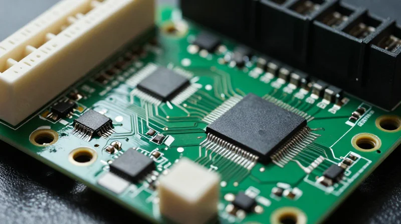
The Architectural Balance of IoT Thermostat PCBs
A high-performance thermostat PCB is defined by the separation and integration of two distinct functional domains: the sensitive analog signal chain and the high-speed digital processing core. Achieving reliable performance requires a stack-up design that minimizes interference, where ground plane integrity and strategic component placement protect low-voltage thermistor readings from the switching noise generated by Wi-Fi radios and microcontrollers.
Core PCB Functional Domains
| Domain | Primary Function | Design Priority |
|---|---|---|
| Analog Sensing | Temperature monitoring | Signal integrity & noise floor |
| Digital Logic | Processing & logic execution | Signal integrity & clock speed |
| RF/Wireless | Connectivity (Wi-Fi/BLE) | Antenna tuning & impedance |
| Power Stage | HVAC relay control | Isolation & creepage distances |
Design Considerations for Mixed-Signal Integrity
- How does layer stack-up impact thermal accuracy?
Improper stack-up can lead to ground bounce or induced noise on sensitive ADC inputs. A 4-layer stack-up is typically recommended to provide dedicated reference planes, which help isolate analog returns from digital switching currents. - Why is isolation critical for relay control?
Since thermostats often switch 24VAC HVAC systems, galvanic isolation between the low-voltage control circuitry and the high-voltage relay coil is mandatory to prevent transient surges from damaging the microcontroller. - What role does thermal relief play in PCB mounting?
To prevent inaccurate temperature readings caused by board heating, sensitive sensors should be physically separated from power-hungry regulators and Wi-Fi modules, utilizing slots or cutouts in the PCB substrate to minimize thermal conductivity.
Optimizing Copper Weight for Thermal Dissipation
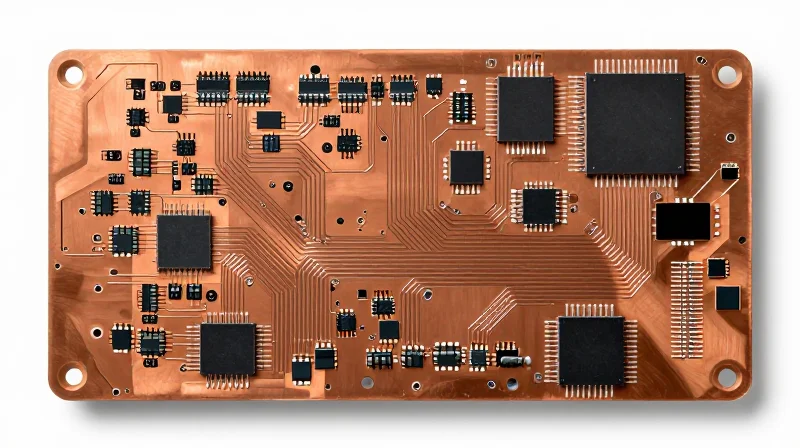
Strategic Copper Weight Selection for Thermal Isolation
In IoT thermostat design, the copper weight directly dictates the thermal resistance of your PCB. While thicker copper (e.g., 2oz) is excellent for heat spreading in power stages, it can inadvertently conduct heat from relay drivers or power regulators toward the ambient temperature sensor. To minimize this, use a baseline of 1oz copper for signal layers while selectively increasing copper weight only in high-current power planes, and employ thermal relief cuts or 'slots' to physically disconnect the thermal conduction path between power components and the sensing area.
Comparison of Copper Weight for Thermal Management
| Copper Weight | Primary Application | Thermal Performance | Risk Profile |
|---|---|---|---|
| 0.5 oz | Fine-pitch digital signaling | Low thermal mass/conductivity | Risk of trace overheating in high current paths |
| 1.0 oz | Standard industry default | Balanced heat dissipation | Ideal for low-power IoT sensing zones |
| 2.0 oz+ | Power conversion and relay drivers | High thermal spreading | Can bias sensors if thermally coupled |
Frequently Asked Questions on Thermal DFM
- How do I prevent power component heat from reaching the sensor?
Implement a thermal moat (a routed slot in the FR4) around the sensor area to break the copper continuity. Additionally, maximize the distance between power inductors and the primary thermistor. - Can I use internal planes to act as a heat sink?
Yes, but be careful. If you connect an internal ground plane to a hot power component, that plane becomes a global heat radiator. Keep the internal copper pour under the sensor electrically connected to ground but thermally isolated from the high-power zones. - What is the impact of Vias on thermal coupling?
Vias are efficient thermal conductors. Avoid placing thermal vias in close proximity to the sensor, as they can pull heat from internal layers directly into the board surface.
Strategic Component Placement for High-Density Boards
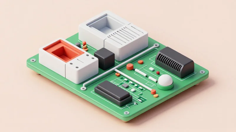
Spatial Partitioning for Signal Integrity and Safety
In space-constrained IoT designs, component placement is governed by the need to isolate high-voltage AC/DC switching circuits—typically handling 24V HVAC control or line voltage—from the precision low-voltage microcontroller (MCU) and analog sensing stages. Effective DFM strategy mandates a 'zonal' layout approach where the PCB is partitioned into a high-energy zone, an intermediate conversion zone, and a quiet logic zone. By maintaining physical separation and utilizing guard traces, designers can mitigate electromagnetic interference (EMI) and prevent switching noise from compromising the accuracy of on-board thermistors.
Clearance Requirements for Power and Logic
| Circuit Type | Clearance Constraint | Reasoning |
|---|---|---|
| High-Voltage AC | Minimum 3.0mm (Creepage) | Prevent dielectric breakdown and arcing |
| Switching Regulator | Minimized Loop Area | Reduce radiated EMI/Inductive coupling |
| Analog Sensing | Isolated Ground Plane | Maintain signal integrity and SNR |
Best Practices for High-Density Layouts
- How should high-voltage components be oriented?
Place high-voltage components, such as relays or triacs, near the board perimeter to ensure adequate creepage distances and allow for simplified routing of high-current paths away from the MCU. - Why is keep-out zone definition critical?
Defining strict keep-out zones under inductors and sensitive analog traces prevents capacitive coupling that could introduce ripples into the thermostat's temperature data, potentially causing false HVAC triggers. - How do you manage heat-generating components?
Place power-heavy components, such as voltage regulators, on the bottom side if possible, or use thermal vias connected to internal ground planes to pull heat away from the sensitive thermistor assembly.
To achieve maximum density without sacrificing reliability, utilize micro-vias and blind-buried vias where feasible. However, ensure that the PCB stackup accommodates the necessary trace widths for current-carrying capacity while respecting standard manufacturer drill-to-copper clearances.
Mitigating Signal Noise in Sensitive Thermistor Circuits

Isolating Analog Sensing from Digital Noise
Thermistor circuits rely on precision voltage dividers, making them highly susceptible to coupling from high-speed digital switching and wireless modules. To maintain measurement accuracy, designers must enforce strict physical separation and implement targeted ground plane strategies to prevent ground bounce and inductive crosstalk from corrupting the sensor feedback.
Critical Routing and Grounding Techniques
- Differential Pair Routing
Route thermistor feedback lines as differential pairs to ensure common-mode noise rejection, even for single-ended signals, by balancing impedance and proximity. - Guard Traces
Surround sensitive analog traces with grounded guard tracks to provide a low-impedance path for induced currents, effectively shielding them from neighboring PWM or RF signals. - Star Grounding
Utilize a star grounding topology where the analog sensor ground connects to the main system ground at a single, clean reference point to prevent digital return currents from traversing the sensitive sensing loop.
| Noise Source | Coupling Mechanism | Primary Mitigation DFM Rule |
|---|---|---|
| PWM Switching | Inductive Crosstalk | Maintain >3x trace width clearance |
| Wireless/RF Modules | Electromagnetic Radiation | Use grounded copper keep-out zones |
| High-Current Loops | Ground Bounce | Dedicated analog ground island |
Best Practices for Filtering
Beyond physical separation, hardware-level filtering is essential. Place a high-quality RC low-pass filter as close to the microcontroller's ADC pin as possible. Ensure that capacitors are rated for the thermistor's operating temperature range and use NP0/C0G dielectric materials to prevent capacitance drift, which would otherwise introduce measurement errors.
/* Recommended RC filter configuration for ADC input */
#define ADC_FILTER_R 1000 // 1k Ohm series resistor
#define ADC_FILTER_C 0.1e-6 // 0.1uF C0G capacitor
// Place these components within 5mm of the MCU pin
Thermal Isolation Design Patterns
Engineering Thermal Isolation Strategies
To achieve high-precision sensing in compact IoT thermostats, engineers must employ physical board-level strategies to decouple the sensor environment from the heat-generating power supply units (PSU) and wireless modules. The primary objective is to maximize thermal resistance between the heat source and the sensor by manipulating the board's substrate and copper topography.
Physical Isolation Patterns
- Thermal Slotting (Air Gaps)
Implement mechanical routing or milling slots between the sensor region and the rest of the PCB. This physically breaks the thermal path through the FR4, significantly reducing conductive heat transfer. - Copper Pour Relief
Remove copper pours and planes around the temperature sensor trace area. By preventing a continuous thermal bridge, you force heat to travel a longer path, effectively acting as a thermal bottleneck. - Thermal Vias and Moats
Utilize 'thermal moats'—a series of non-plated holes or a perimeter of isolation—to force heat around the periphery of the board rather than allowing direct flow toward the sensor input stage.
Design Pattern Comparison Table
| Design Pattern | Complexity | Thermal Efficacy | Manufacturing Impact |
|---|---|---|---|
| Mechanical Slotting | High | Maximum | Requires secondary milling |
| Copper Relief | Low | Moderate | No extra cost |
| Component Standoff | Medium | High | Requires specific packaging |
Implementation Best Practices
When designing the PCB layout, always consider the thermal coefficient of expansion (TCE) if using rigid-flex or specific board substrates. For sensors requiring high accuracy, ensure the sensor is placed on a 'thermal island' connected to the main PCB via thin, narrow traces that minimize conductive surface area, thereby limiting heat ingress from the main electronics.
DFM Rules for Automated Assembly (SMT)
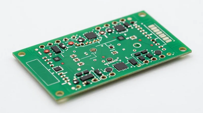
Essential SMT Design for Manufacturing Rules
Automated assembly efficiency relies heavily on predictable board handling and component placement. For IoT thermostat boards, which often feature small, high-density components, rigid adherence to DFM standards for fiducials, panelization, and solder masks is critical to reducing rework and production downtime.
Fiducial Standardization
Fiducials act as the global and local reference points for automated optical inspection (AOI) and pick-and-place systems. Inaccurate or missing fiducials will lead to placement errors on fine-pitch components like Wi-Fi modules or low-power MCUs.
- Global Fiducials
Place at least three fiducials on the panel frame for orientation, with two placed in non-symmetrical corners to prevent board reversal errors. - Local Fiducials
Required for fine-pitch components (pitch < 0.5mm). Place these on the board near the component to ensure local accuracy. - Clearance Requirements
Maintain a clear zone around fiducials at least twice the diameter of the mark to prevent interference from silk-screen or nearby traces.
Panelization and Handling
Effective panelization optimizes material usage and ensures smooth conveyor travel through the assembly line. Tab-routing with breakaway tabs is preferred over V-scoring for small, irregular thermostat shapes to prevent mechanical stress during depanelization.
| Feature | Recommended Practice | Benefit |
|---|---|---|
| Edge Clearance | 3mm - 5mm rail | Secure gripping by SMT conveyors |
| Component Spacing | > 2mm from edge | Prevents mechanical damage |
| Depanelization | Routed tabs | Reduces board warping/stress |
Solder Mask Design and Stencil Optimization
Solder mask registration and aperture design determine the reliability of solder joints on miniaturized IoT sensors. Excessive mask-to-pad overlap can lead to tombstoning of 0201 or 0402 components due to uneven wetting forces.
- Mask Opening Ratio
Design solder mask openings to be 0.1mm larger than the pad size to allow for manufacturing registration tolerances. - Stencil Design
Use laser-cut electro-polished stencils with an aperture-to-pad ratio of 1:1 for fine-pitch parts to maintain solder volume consistency. - Via-in-Pad
If using via-in-pad for space-constrained designs, ensure vias are filled and capped to prevent solder wicking and resulting voids.
Material Selection and Stack-up Considerations
Substrate Selection for HVAC Reliability
Selecting the correct PCB substrate is the foundation of long-term reliability in thermostat applications, where boards undergo repetitive thermal cycling and potential moisture exposure. While Standard FR-4 is sufficient for basic consumer electronics, IoT thermostats benefit from High-Tg (Glass Transition Temperature) FR-4 materials to maintain structural integrity when internal enclosures heat up near switching relays or power components.
| Material Type | Tg Value | Recommended Application | Cost Profile |
|---|---|---|---|
| Standard FR-4 | 130-140°C | Basic logic/display boards | Lowest |
| Mid-Tg FR-4 | 150-170°C | IoT sensors/Wireless modules | Moderate |
| High-Tg FR-4 | >170°C | Relay-heavy HVAC controllers | Premium |
Strategic Stack-up Considerations
A balanced stack-up is essential to prevent PCB warpage during assembly and operation. By keeping the stack-up symmetrical around the center axis, engineers minimize internal stress caused by varying coefficients of thermal expansion (CTE). For IoT thermostats, a 4-layer stack-up is generally the sweet spot, allowing for a dedicated ground plane to mitigate EMI from onboard Wi-Fi or Bluetooth radios.
- Why is symmetry important in stack-up?
A symmetrical layer arrangement ensures even thermal expansion and contraction, preventing the board from bowing or twisting during reflow soldering or field use. - Should I use internal copper planes?
Yes, utilizing internal layers for solid ground and power planes provides a low-impedance path for current and enhances shielding for sensitive thermistor analog signals. - How do I balance cost and thermal stability?
Specify 1oz copper for signal layers and 1.5oz or 2oz for high-current relay tracks to allow for thinner overall board profiles without sacrificing thermal performance.
Rigorous Validation and Testing Frameworks
Post-Manufacturing Testing Protocols
Reliability in IoT thermostats starts with comprehensive verification strategies that detect manufacturing defects before field deployment. For high-volume control boards, the combination of In-Circuit Testing (ICT) and Flying Probe Testing provides a robust defense against electrical shorts, opens, and component misplacement.
| Test Method | Best For | Key Advantage |
|---|---|---|
| ICT (Bed-of-Nails) | High-volume production | Rapid cycle times and comprehensive coverage |
| Flying Probe | Low-to-mid volume / Prototypes | No expensive custom fixture required |
| Thermal Stress | Field longevity validation | Detects latent defects in extreme conditions |
Thermal Stress and Environmental Validation
Given that thermostats function in diverse climatic conditions, thermal chamber stress testing is non-negotiable. Subjecting boards to accelerated aging through repeated thermal cycling ensures that solder joints and component interconnects can withstand the expansion and contraction cycles typical of seasonal HVAC operation.
Testing Best Practices FAQ
- How does Flying Probe reduce DFM costs?
It eliminates the need for a dedicated test fixture, allowing for iterative board design changes without incurring high re-tooling costs. - What is the role of ICT in high-volume manufacturing?
ICT verifies every net and component value, ensuring that automated assembly lines are performing consistently and identifying individual board defects in milliseconds. - Why is thermal cycling required for IoT thermostats?
It exposes infant mortality defects in passive components and stress-related solder failures that do not manifest during standard room-temperature electrical testing.
Mastering these DFM rules is essential for minimizing manufacturing defects and maximizing product precision in the competitive IoT market. By prioritizing thermal isolation and trace integrity early in the design cycle, your team can accelerate time-to-market. Ready to optimize your hardware? Contact our engineering team today for a comprehensive design audit of your latest control board project.
