
Developing high-performance smart plugs requires navigating the narrow intersection of severe space constraints and robust RF reliability. As device footprints shrink, engineers often struggle with signal interference and thermal dissipation. This article provides the blueprint for mastering these challenges through rigorous DFM protocols and precise antenna integration.
The Challenge of Miniaturization in Smart Plug Design
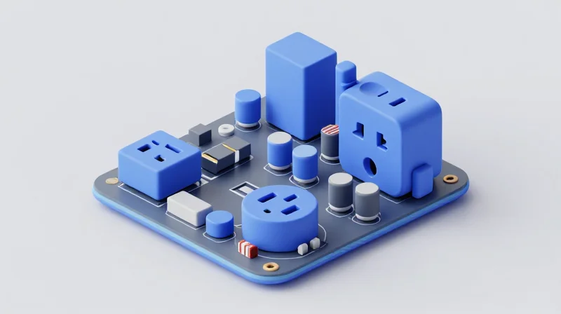
The Triad of Miniaturization Constraints
Miniaturizing smart plug electronics is fundamentally a battle against the physics of power density. As consumer demand for sleeker, non-obstructive form factors increases, engineers are forced to compress AC-DC conversion circuitry, high-current relay modules, and RF communication modules into tight volumes. This architectural shift significantly limits airflow, complicating heat dissipation, and forces higher component density, which exacerbates electromagnetic compatibility (EMC) challenges.
Critical Engineering Challenges
- Thermal Management
Internal temperature rise in confined housings can degrade capacitors and weaken solder joints, necessitating high-efficiency switching topologies and strategic placement of power components away from the WiFi SoC. - Creepage and Clearance
Adhering to safety standards like UL or IEC while shrinking the PCB footprint requires meticulous trace routing to maintain mandated distances between high-voltage AC paths and low-voltage control circuitry. - RF Interference
The proximity of high-frequency switching noise from the power supply to the sensitive WiFi radio front-end frequently leads to degraded signal integrity if effective shielding and layout isolation are not prioritized.
Design Trade-off Matrix
| Design Factor | Miniaturization Impact | Mitigation Strategy |
|---|---|---|
| Power Density | Higher heat generation | Use GaN semiconductors/high-efficiency components |
| Component Spacing | Reduced safety clearances | Vertical stacking and slot milling |
| WiFi Range | Increased noise floor | Dedicated board-level shielding |
Ultimately, successful miniaturization in smart plug design is not about simply shrinking parts; it is about managing the increased power density through rigorous thermal modeling and electromagnetic isolation. Failure to address these constraints at the schematic capture and board layout stage often leads to repeated certification failures and long-term product unreliability.
Foundational DFM Protocols for Compact Enclosures
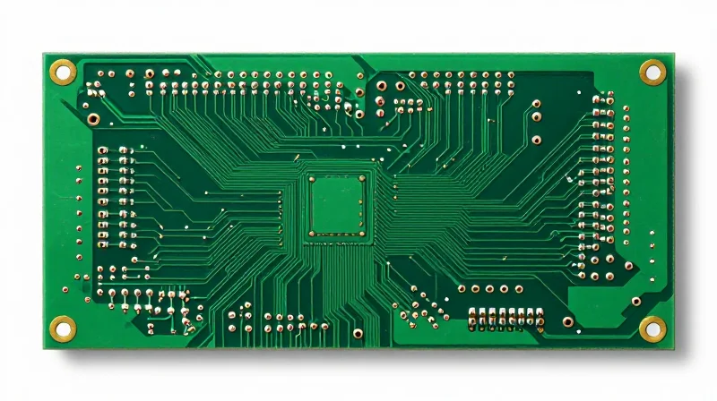
Optimizing Board Edge Clearance and Layout Density
In compact smart plug enclosures, PCB real estate is highly constrained. To ensure high-yield SMT assembly, developers must enforce strict clearance rules, particularly around the high-voltage AC mains input and the isolated low-voltage control circuitry. Maintaining a minimum edge clearance of 0.5mm is essential to prevent PCB routing damage during the singulation process and to ensure adequate creepage for safety certifications.
| Parameter | Recommended Constraint | Rationale |
|---|---|---|
| Board Edge Clearance | 0.5mm minimum | Singulation safety and handling |
| Component-to-Component | 0.25mm | SMT nozzle access and rework |
| Copper-to-Board Edge | 0.3mm | Prevention of shorts/arcing |
Managing Manufacturing Tolerances in Dense Assemblies
As component density increases, manufacturing tolerances become the deciding factor between a reliable product and a high failure rate. Relying on tighter tolerances for pick-and-place precision is insufficient; you must design with 'robustness by default' by optimizing pad stacks for secondary reflow operations.
- How do I mitigate stencil clogging with high-density components?
Use electro-polished stencils with optimized aperture ratios and ensure component orientation is perpendicular to the wave solder direction if dual-wave processes are employed. - Why is trace width critical in high-density smart plugs?
Beyond signal integrity, narrow traces in power paths increase localized heating, potentially compromising the thin-walled plastic enclosure during long-term operation. - What is the best strategy for component orientation?
Align all polarized components in the same direction to simplify AOI (Automated Optical Inspection) and reduce errors in the pick-and-place programming phase.
Thermal Relief and Copper Balancing
Thermal management in small enclosures requires intentional copper balancing. Uneven copper distribution leads to board warping during reflow, causing intermittent contact issues in the WiFi module's surface-mount connectors. Always apply thermal relief pads for components connected to large planes to ensure consistent solder joint quality while maintaining the thermal path necessary for heat dissipation.
Optimizing WiFi Antenna Placement for Signal Integrity

Achieving reliable wireless connectivity in a compact smart plug requires a rigorous approach to antenna integration. The primary challenge lies in balancing the proximity of high-frequency WiFi signals with noisy AC-DC switching power supplies and high-current relay switching, which can introduce significant EMI and desensitize the receiver.
Mitigating Interference from Power Electronics
Power components act as primary noise sources. To maintain signal integrity, maintain a minimum physical clearance (the 'keep-out zone') between the antenna and the switching regulator. Avoid routing high-speed digital signals or high-current AC paths directly beneath the antenna area.
| Interference Source | Impact | Mitigation Strategy |
|---|---|---|
| Switching Regulators | Wideband noise floor increase | Shielding and physical distancing |
| Relay Actuation | Transient spikes/EMI | Snubber circuits and distance |
| AC Power Traces | Magnetic field interference | Keep-out area (min 10mm) |
Antenna Placement and Enclosure Dynamics
Placement within the plastic housing is critical for radiation pattern symmetry. Ensure the antenna is placed as far as possible from the grounded metal components of the plug pins and internal heatsinks, which can act as Faraday cages if placed improperly.
- Why is the antenna keep-out zone vital?
Any copper planes, traces, or metal components within the antenna's near-field zone will shift the resonant frequency and reduce radiation efficiency. - Should I use an onboard trace antenna or an external chip?
Onboard PCB trace antennas are cost-effective but sensitive to layout geometry; ceramic chip antennas are smaller and more predictable, making them better for extremely tight smart plug enclosures. - Does plastic thickness matter?
Yes, dense or metallic-paint-coated plastics can significantly attenuate 2.4GHz signals, creating a 'dead zone' around the device.
Multi-Layer PCB Stackup Strategies for IoT Devices
Strategic Stackup for Miniaturized IoT Hardware
In the confined environment of a smart plug, a 4-layer stackup is typically the minimum requirement to balance signal integrity with noise isolation between high-voltage AC mains and sensitive low-voltage wireless circuitry. By employing a signal-ground-ground-signal configuration, designers can effectively isolate RF traces from switching noise while maintaining a low-impedance path for return currents.
Layer Allocation and Signal Integrity
| Layer | Function | Purpose |
|---|---|---|
| L1 (Top) | RF/Analog | Shortest path for WiFi antenna and low-voltage signal routing. |
| L2 (Internal) | GND Plane | Continuous return path; shields RF signals from power noise. |
| L3 (Internal) | Power/GND | Localized power distribution for MCU and relay control. |
| L4 (Bottom) | High Voltage/AC | AC line routing, kept away from sensitive digital inputs. |
Mitigating EMI and Noise Coupling
To prevent switching transients from AC power electronics from corrupting WiFi performance, the internal GND plane must remain unbroken. Designers should adopt a 'split-zone' approach, where the high-voltage section is physically separated from the RF section on the board, bridged only by opto-isolators or low-capacitance transformers.
FAQs for Multi-Layer Stackup Design
- Why is a 4-layer board preferred over 2-layer?
A 4-layer board provides a dedicated reference plane for signals, significantly reducing radiated emissions and improving impedance control for the WiFi antenna. - How should I handle the thermal vias?
Place high-density thermal via arrays under power-switching components to sink heat into the internal copper planes, which act as secondary heatsinks. - Should the GND planes be connected?
Use a single-point 'star' ground strategy to prevent large AC return currents from flowing through the sensitive ground plane shared by the wireless SoC.
Mitigating Electromagnetic Interference (EMI) and Noise
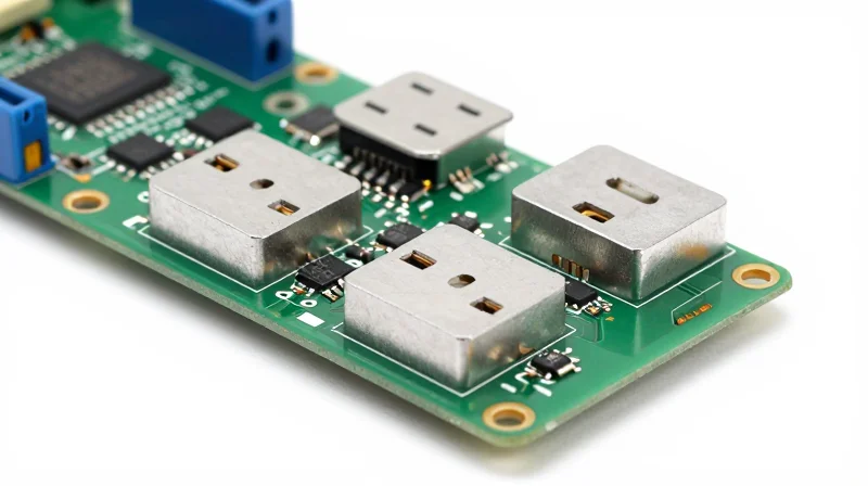
Managing Noise in Compact Smart Plug PCBA Designs
Smart plugs inherently pair noisy AC-to-DC switching power supplies with sensitive RF front-end circuitry on a single, cramped PCB. To mitigate interference, designers must implement strict physical separation between the high-voltage mains input and the low-voltage logic section. By maintaining a clean ground plane and utilizing localized filtering for switching nodes, developers can prevent high-frequency noise from coupling into the WiFi module's reference clock and antenna.
Techniques for EMI Suppression and Compliance
| Mitigation Strategy | Implementation Technique | Regulatory Impact |
|---|---|---|
| Switching Node Isolation | Short traces, minimal copper area | Reduces radiated EMI (FCC Part 15) |
| Common-Mode Filtering | Chokes on AC input traces | Lowers conducted emissions |
| Shielding Cans | Metal cages over RF circuits | Prevents crosstalk and spurious emissions |
Frequently Asked Questions on Noise Isolation
- How does PCB stackup influence EMI?
A high-quality stackup utilizes a dedicated inner ground plane beneath the RF and power stages. This provides a low-impedance return path that contains signal loops, drastically reducing radiated emissions. - Should I use ferrite beads for WiFi modules?
Yes. Placing ferrite beads on the VCC lines leading to the wireless module effectively suppresses high-frequency noise originating from the switching power supply before it impacts sensitive signal integrity. - Why is keep-out zone design critical?
Proper keep-out zones around the antenna and high-speed switching nodes prevent parasitic capacitance from coupling noise into the antenna, ensuring the device remains within CE/FCC sensitivity requirements.
Thermal Management in Enclosed AC-to-DC Designs

Thermal Management Strategies for Compact PCBA
In the confined environment of a smart plug, heat dissipation is constrained by limited convection and the proximity of high-frequency power electronics to the WiFi module. Managing thermal load begins with board layout; high-power components such as the AC-to-DC converter MOSFETs and bridge rectifiers should be placed to ensure the heat path is directed away from the RF antenna and sensitive logic ICs.
Optimizing Heat Dissipation Techniques
- Thermal Vias and Copper Pours
Utilize extensive copper pours on internal layers to act as heat spreaders. Implement a dense grid of thermal vias beneath hot components to conduct heat effectively to the bottom layers of the PCB, increasing the effective surface area for dissipation. - Component Derating
Always derate power components relative to the maximum ambient temperature expected within the closed enclosure. Designing for a 20-30% margin in power handling reduces the baseline heat generation of the circuit. - PCB Material Selection
For high-density designs, consider using high-TG (glass transition temperature) FR4 laminates to ensure mechanical and thermal stability under prolonged heating cycles.
| Thermal Strategy | Implementation Priority | Primary Benefit |
|---|---|---|
| Copper Pour Spreading | High | Increases effective surface area |
| Thermal Via Stitching | High | Reduces junction-to-ambient resistance |
| Component Isolation | Medium | Protects sensitive RF components |
Design Considerations for Enclosure Integration
The enclosure material and vent design are critical final barriers to thermal failure. While aesthetic requirements often demand seamless plastics, engineers must integrate discreet ventilation channels or utilize internal thermal pads to bridge the gap between heat-generating components and the plastic chassis to facilitate heat sinking. Avoid placing the WiFi module directly behind power components; instead, position it near the ventilation ports to leverage ambient airflow while maintaining signal integrity.
DFM Checklist for Prototype to Production
DFM Verification Checklist
Transitioning to mass production requires moving beyond mere functionality to emphasize assembly yield, cost-optimization, and long-term reliability under AC mains stress.
- Component Sourcing Stability
Verify that all critical components, specifically the Wi-Fi SoC, AC-DC controller, and relay, have long-term availability and multiple authorized distributors to avoid supply chain bottlenecks. - Panelization Efficiency
Optimize PCB dimensions for panel utilization; target standard panel sizes (e.g., 18x24 inches) to reduce waste and lower the per-board manufacturing cost. - Test Point Strategy
Integrate comprehensive test points for ICT (In-Circuit Testing) and FCT (Functional Testing) to automate the verification of power regulation, Wi-Fi signal strength, and relay switching logic on the production line. - Thermal Margin Validation
Perform final thermal profiling at maximum rated load in the actual plastic housing to ensure the relay and power supply components do not exceed safety temperature limits during prolonged operation.
Prototype vs. Production Comparison
| Feature | Prototype Focus | Production Focus |
|---|---|---|
| Component Selection | Fast availability/Ease of solder | Cost, lifecycle, and second-sourcing |
| Testing | Manual bench testing | Automated ICT/FCT fixtures |
| Assembly | Hand-soldered/Manual rework | DPMO reduction/Reflow optimization |
| Housing | 3D-printed/Modified off-the-shelf | Injection-molded/Ultrasonic welding |
Quality Control and Compliance
Beyond PCB layout, ensure that the final assembly process includes rigorous end-of-line testing for dielectric withstand (Hi-Pot) and ground continuity. These steps are mandatory for safety certification (UL/ETL) and are non-negotiable for products interfacing with high-voltage AC.
Successfully engineering a compact smart plug requires a meticulous balance between electrical performance and mechanical constraints. By adopting these DFM and RF best practices, you can significantly reduce development cycles and field failures. Contact our engineering team today to optimize your next IoT PCBA project for market-leading reliability.
