In the intricate world of electronics, the through-hole PCB stands as a foundational technology, much like the roots of a tree supporting its branches. This method of mounting components, where leads are inserted through drilled holes, has been the backbone of countless electronic devices for decades. This article delves into the core of through-hole PCB technology, exploring its design principles, assembly processes, and its place in modern electronics alongside newer methods like SMT, providing a comprehensive guide for both newcomers and experienced professionals.
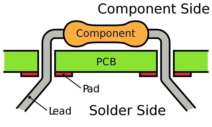
Through-hole technology (THT) is a fundamental method in electronics manufacturing where component leads are inserted into pre-drilled holes on a printed circuit board (PCB) and subsequently soldered in place. This method, one of the earliest PCB assembly techniques, provides robust mechanical connections and secure electrical paths.
The historical roots of through-hole technology lie in the early days of electronics manufacturing when circuit boards were largely hand-assembled. Components with leads extending from their bodies were inserted into holes and then soldered on the opposite side to secure them. This method proved effective for both prototyping and mass production and continues to be utilized today.
The core principle of THT involves creating a physical connection between a component and a PCB through drilled holes, which are typically plated to enhance electrical conductivity. The component lead is passed through the hole and soldered to the pad on the opposite side of the board, establishing both an electrical and mechanical bond.
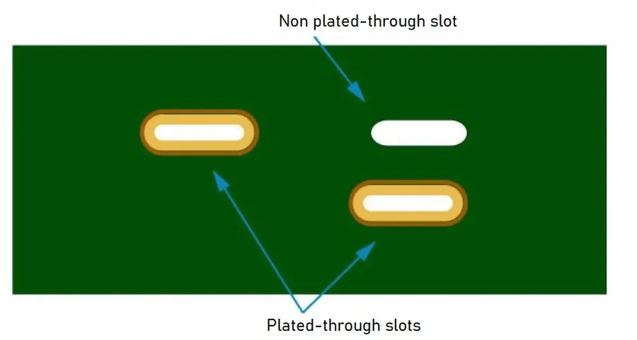
Printed Circuit Boards (PCBs) utilize both Plated Through-Holes (PTH) and Non-Plated Through-Holes (NPTH), each serving distinct purposes crucial to PCB functionality. PTHs provide electrical connectivity between different layers of a multi-layered PCB, while NPTHs are primarily used for mechanical mounting or alignment, without electrical connection. Understanding their differences is fundamental for effective PCB design and assembly.
| Feature | Plated Through-Hole (PTH) | Non-Plated Through-Hole (NPTH) |
|---|---|---|
| Electrical Connection | Yes, provides vertical electrical pathways between layers | No, does not facilitate electrical conductivity |
| Plating | Hole walls are plated with conductive material (e.g., copper) | Hole walls are not plated, typically bare substrate material |
| Primary Function | Electrical interconnection and component mounting | Mechanical mounting, alignment, or clearance |
| Usage | For component leads, vias, and interlayer connections | For mounting hardware, locating pins, or structural support |
| Cost | Higher, due to the additional plating process | Lower, as it avoids the plating process |
The choice between PTH and NPTH depends heavily on the specific requirements of the PCB design. PTH is indispensable in multi-layer PCBs for ensuring reliable electrical connections across different layers. In contrast, NPTHs are selected when electrical conductivity is not required and when mechanical stability is paramount. For example, mounting holes for securing a PCB within an enclosure typically utilize NPTH to save on manufacturing cost and complexity.
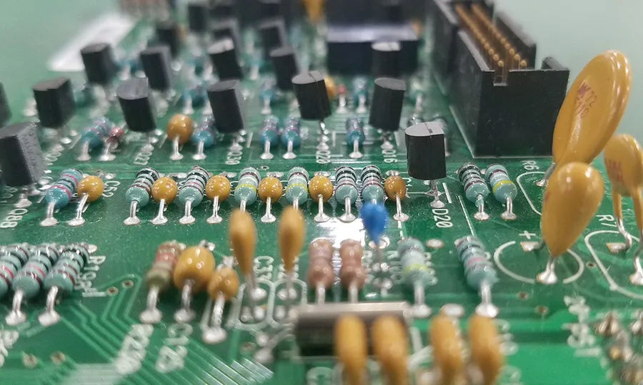
The assembly of through-hole PCBs is a structured process that, when followed carefully, ensures reliable electrical connections and mechanical stability. This section details each step, from preparing components to the final soldering and inspection.
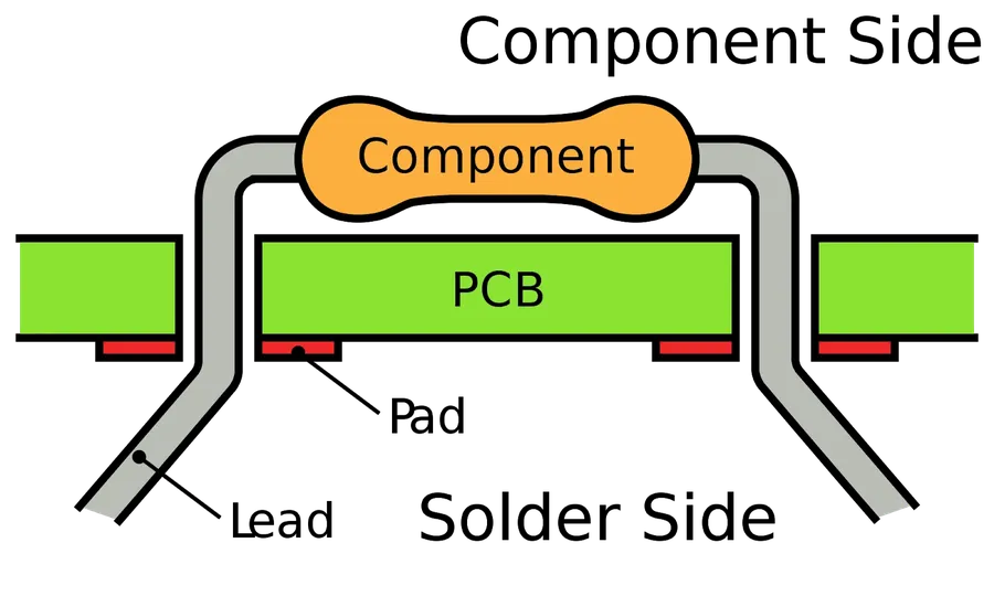
Designing reliable and functional through-hole PCBs necessitates adherence to specific rules and careful consideration of various factors. These guidelines ensure proper component placement, secure mechanical mounting, and optimal electrical performance. Key considerations include hole size, pad design, and component spacing, each directly impacting the manufacturability and long-term reliability of the final product. Ignoring these rules can lead to assembly issues, decreased performance, and even catastrophic failures.
| Design Rule | Description | Importance |
|---|---|---|
| Hole Diameter | The size of the drilled hole for component leads. | Ensures proper component fit and solder joint integrity. Insufficient clearance can damage leads during insertion; excessive clearance can lead to poor solder joints. |
| Pad Size and Shape | The copper area surrounding the hole, for soldering. | Critical for solder joint strength and thermal dissipation. Optimizing shape and size ensures reliable electrical connection and prevents issues such as tombstoning during reflow. |
| Pad to Trace Clearance | The space between the pad and any adjacent copper traces. | Prevents short circuits and ensures proper electrical isolation. Insufficient clearance can lead to unintended current paths and device malfunction. |
| Component Spacing | The physical distance between adjacent through-hole components. | Facilitates manual and automated assembly, ensuring sufficient clearance for tools and preventing interference. Adequate space also allows for rework, if needed. |
| Drill Registration | The accuracy of hole placement during drilling. | Ensures that holes align correctly with component leads and pads. Poor registration can cause manufacturing defects and assembly challenges. |
| Annular Ring | The width of copper pad surrounding a plated through-hole (PTH) after drilling | Ensures electrical connection and mechanical strength. It prevents the drill hole from breaking through the copper pad and guarantees a reliable solder joint. |
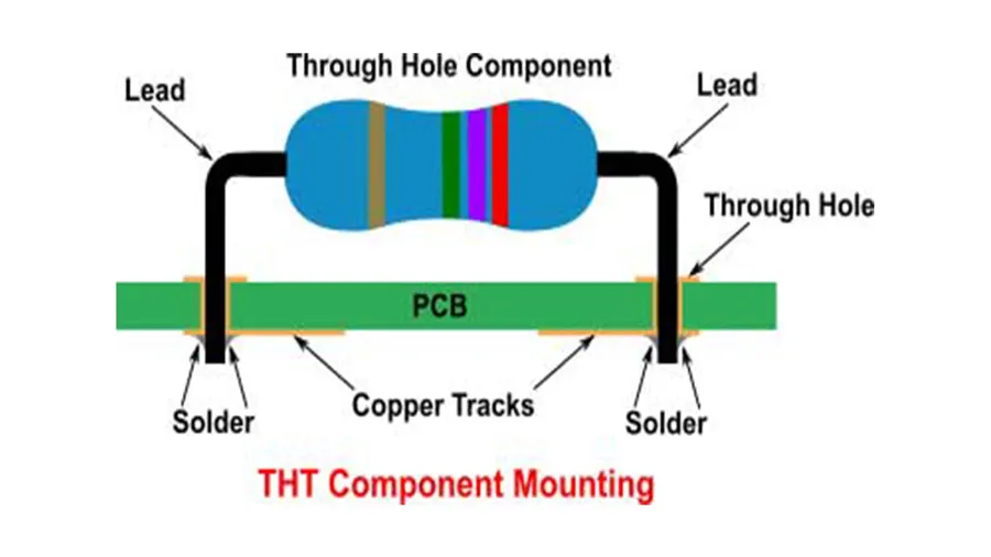
Through-hole components, characterized by their leads that are inserted into drilled holes on a PCB and soldered on the opposite side, are fundamental to electronics design and assembly. This technology allows for robust mechanical connections, making it suitable for applications requiring high reliability and durability. This section details the diverse types of through-hole components and their specific applications, highlighting their advantages in various electronic systems.
| Component Type | Description | Typical Applications | Advantages |
|---|---|---|---|
| Resistors | Passive components that provide a specific resistance to current flow. Commonly used for current limiting, voltage division, and signal termination. | Power supplies, amplifier circuits, signal processing units. | Wide range of resistance values, robust handling, easy to test |
| Capacitors | Passive components that store electrical energy in an electric field. Used for filtering, energy storage, and timing circuits. | Power smoothing, signal coupling, bypass circuits, filter circuits. | Variety of capacitance values, different dielectric materials available |
| Diodes | Semiconductor devices that allow current flow in one direction. Used for rectification, signal detection, and voltage regulation. | Rectifier circuits, voltage clamps, signal demodulation. | Robust and reliable, good for high-voltage and high-current circuits |
| Transistors | Semiconductor devices used to amplify or switch electronic signals and electrical power. Used as amplifiers and switches. | Amplifier stages, switching power supplies, logic circuits. | Versatile for analog and digital applications |
| Integrated Circuits (ICs) | Complex circuits fabricated on a single semiconductor chip. Perform specific functions such as microprocessing, memory management, and signal conditioning. | Microcontrollers, memory modules, logic gates, op-amps. | High integration density, complex functionality |
| Connectors | Devices that facilitate the joining of electronic circuits and other hardware. Allow for modular designs and easy replacement of parts. | Input/output interfaces, power connections, board-to-board connections. | Variety of connection types available for specific functions, robust connections |
| Inductors | Passive components that store energy in a magnetic field. Used for filtering, tuning circuits, and impedance matching. | Power supplies, resonant circuits, filter circuits. | Good for high-current applications, variety of inductance values |
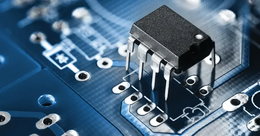
Through-hole technology (THT) and surface mount technology (SMT) represent the two dominant methods for mounting electronic components onto printed circuit boards (PCBs). This section provides a direct comparison of these two technologies, analyzing their respective strengths, weaknesses, and application suitability, thereby enabling engineers to make informed decisions based on their project requirements.
| Feature | Through-Hole Technology (THT) | Surface Mount Technology (SMT) |
|---|---|---|
| Component Mounting | Component leads inserted into drilled holes on PCB. | Components soldered directly onto the surface of PCB. |
| Mechanical Strength | Provides high mechanical strength due to component leads through the board. | Generally lower mechanical strength but can be improved by robust pad design and materials. |
| Assembly Process | Requires manual or automated through-hole insertion and soldering. | Highly automated pick-and-place and reflow soldering process. |
| Component Size | Generally larger components, often with leaded packages. | Allows for miniaturized components and high-density designs. |
| Component Density | Lower component density due to space required for holes and leads. | Higher component density on PCB enabling miniaturization of the design. |
| Manufacturing Cost | Higher cost for mass production due to the need for drilling and through-hole component mounting. | Lower cost for mass production due to automated assembly process and standardized components. |
| Thermal Performance | Better thermal performance for high-power devices due to component leads acting as heat sinks. | Requires careful thermal design, especially for power-intensive applications. |
| Ease of Prototyping | More suitable for prototyping and hobbyist projects due to ease of manual assembly. | Can be more challenging for prototyping without specialized equipment. |
| Rework and Repair | Easier to rework and repair using standard soldering equipment. | Requires specialized equipment and expertise for rework. |
| Applications | Suitable for robust applications where mechanical strength is critical, and for prototyping and hobbyist use. | Ideal for mass-produced consumer electronics, high-density designs and high frequency designs. |
This section addresses common queries regarding through-hole PCB technology, offering clear explanations and comparisons to surface mount technology (SMT). It aims to resolve any uncertainties and provide a solid understanding of through-hole PCB design and application.
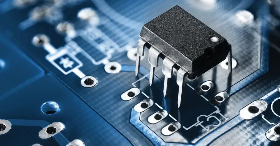
While surface mount technology (SMT) dominates modern electronics, through-hole technology continues to thrive in specialized and high-reliability applications. Its inherent robustness and mechanical strength offer distinct advantages where physical durability is paramount. This section will explore these niche applications and speculate on the future evolution of through-hole technology.
Through-hole components are still heavily utilized in several critical sectors, particularly where robust connections and high power handling are essential. These applications leverage the physical strength of through-hole mounting, providing a far more secure connection than SMT components in demanding operating environments. As technology continues to evolve, through-hole maintains its relevance and applicability in areas where absolute reliability and durability are key requirements.
Looking ahead, while SMT continues to dominate in miniaturization, the longevity of through-hole technology remains secured by its inherent advantages. The future will likely see a consolidation of through-hole applications within those areas requiring its distinct advantages, while SMT will continue in the mass production of portable electronics. A future trend may see materials development to enhance through-hole components' high temperature and vibrational tolerance even further.
The future of through-hole technology may also see the development of hybrid mounting techniques combining the strengths of both SMT and through-hole on a single board. Such boards may utilise SMT for standard components and reserve through-hole mounting for critical and higher power components. The future will likely see a synergistic approach to PCB design that leverages both SMT and through-hole technologies.
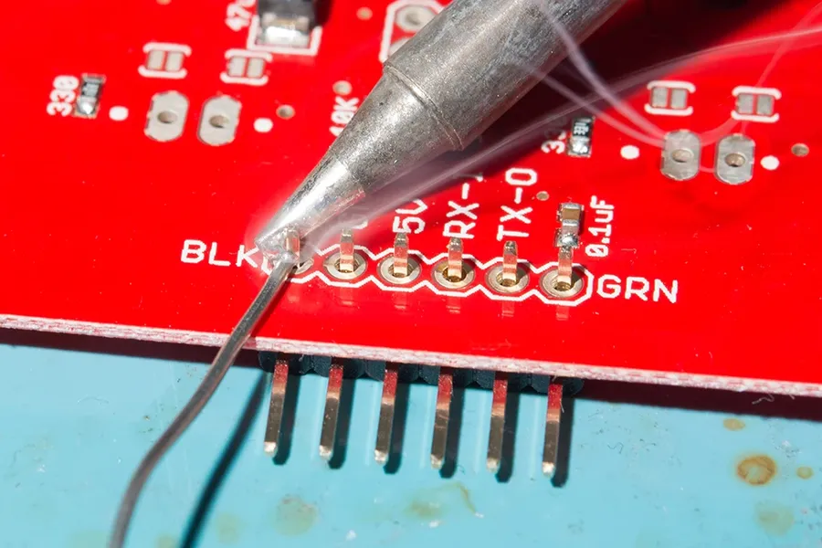
Ensuring high-quality soldering for through-hole components is crucial for the reliability and longevity of electronic devices. This section outlines essential techniques and inspection methods to achieve robust solder joints and avoid common soldering pitfalls.
Through-hole PCB technology, despite the rise of SMT, remains a critical part of electronic manufacturing, offering robustness and reliability where it matters most. Understanding its nuances, from design principles to assembly techniques, is essential for anyone involved in PCB development. This guide provides a foundational knowledge, with practical insights and considerations for leveraging the full potential of through-hole technology in modern electronic designs. As we continue to innovate, it is crucial to recognize the legacy and ongoing value of this foundational method.

