
In the fast-paced world of high-volume electronics, the gap between a prototype and a profitable product often lies in the assembly line. Every inefficient design choice creates a compounding tax on your bottom line, manifesting as scrap, rework, or extended cycle times. This article explores how meticulous DFM application transforms digital thermometer production from a logistical challenge into a streamlined, high-yield engine for growth.
The Strategic Importance of DFM in High-Volume PCBA

Defining DFM as a Financial Lever
In the context of high-volume digital thermometer production, Design for Manufacturing (DFM) is not merely a technical guideline; it is a strategic financial instrument. By integrating manufacturing constraints into the initial design phase, engineering teams can proactively eliminate costly assembly bottlenecks before a single board is populated. This front-loading of design intelligence ensures that the PCBA architecture is optimized for automated pick-and-place precision, reducing scrap rates and accelerating time-to-market.
DFM vs. Traditional Design Impacts
| Feature | Traditional Design | DFM-Optimized Design |
|---|---|---|
| Component Selection | Performance-centric only | Supply chain & cost-optimized |
| Assembly Speed | Lower (Manual intervention) | Higher (Automated throughput) |
| Yield Rates | Inconsistent | Highly predictable |
Core Principles for Scaling Production
- How does DFM affect long-term unit costs?
DFM lowers unit costs by reducing cycle times, minimizing the need for manual rework, and utilizing standardized, readily available components that leverage economies of scale. - Why is early involvement of the manufacturing team vital?
Manufacturing experts provide real-world insights into assembly tolerances and equipment limitations, preventing the 'over-engineering' trap that leads to higher production overhead. - Can DFM improve product reliability in digital thermometers?
Yes, by enforcing layout standards that prevent thermal stress and signal interference, DFM practices directly contribute to higher field reliability and reduced warranty costs.
Case Study Analysis: The Digital Thermometer Production Bottleneck

The Challenge: Identifying the Thermometer Sensor Bottleneck
During the initial scale-up of a high-volume digital thermometer project, the manufacturing facility experienced a 14% rejection rate at the final sensing unit integration stage. Root cause analysis revealed that the original PCBA layout forced high-precision thermistor placement into a congested zone, causing thermal stress during the reflow process and misalignment during pick-and-place.
Impact on Production Metrics
| Metric | Pre-Optimization | Post-Optimization |
|---|---|---|
| Rejection Rate | 14.2% | 0.8% |
| Throughput (Units/Hour) | 450 | 820 |
| Average Unit Cost | $2.45 | $1.98 |
Engineering Solutions and Process Refinements
To mitigate these failures, the engineering team implemented a multi-stage rectification strategy. By introducing fiducial markers closer to the sensor pad and adjusting the copper pour to prevent uneven heat dissipation, the team achieved stability in the reflow profile.
- How did layout changes improve yield?
Redesigning the trace routing prevented thermal mass imbalances, significantly reducing micro-cracks in the sensor solder joints. - Why was the reflow profile adjustment critical?
The original profile was too aggressive for the delicate thermistor components; slowing the ramp-up phase protected sensitive internal structures from thermal shock. - What role did automated optical inspection (AOI) play?
By updating AOI algorithms to detect minute offsets in thermistor positioning, the team caught defects earlier, preventing wasted upstream assembly time.
Conclusion on ROI Impact
By addressing the PCBA layout issues during the early manufacturing phase, the firm reduced scrap costs by 94% and increased global shipping volume by nearly 80%. This case demonstrates that small adjustments in design for manufacturing directly correlate to massive improvements in profitability and market scalability.
Component Selection and Standardization for Cost Efficiency
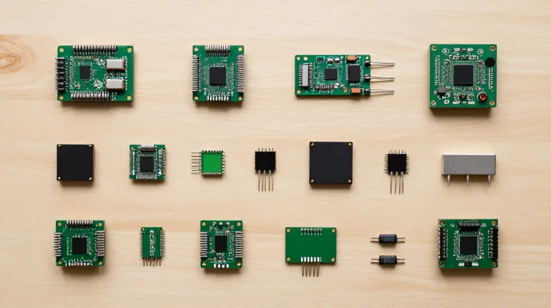
Component Selection and Standardization for Cost Efficiency
In the high-volume production of digital thermometers, the proliferation of unique components is the primary driver of supply chain complexity and escalating overhead. By enforcing a strict policy of component consolidation and prioritizing industry-standard footprints (such as 0402 or 0603 passives), manufacturers can consolidate procurement volumes, negotiate volume discounts, and reduce the risk of line stoppages due to individual component shortages.
Strategic Advantages of Standardized Footprints
| Parameter | Custom/Proprietary Components | Standardized Footprints |
|---|---|---|
| Procurement Lead Time | Variable/Long | Immediate/Off-the-shelf |
| Unit Cost | High (Limited Vendors) | Low (Commoditized) |
| Quality Stability | Dependent on Single Source | Proven Multi-Vendor Reliability |
| Assembly Speed | Requires Specialized Tooling | Optimized for High-Speed SMT |
Implementation Best Practices
To effectively scale, engineering teams must transition from 'best-in-class' selection to 'common-in-class' selection. This involves auditing the Bill of Materials (BOM) to eliminate redundant components that serve identical functions. Utilizing a unified library of components approved by both engineering and sourcing departments prevents the introduction of low-volume parts that complicate inventory management.
- How does component consolidation impact SMT throughput?
Standardizing footprints reduces the need for frequent nozzle or feeder changes on placement machines, significantly increasing the net board throughput during high-speed assembly. - What is the ROI of using multi-sourced standard passives?
Using standard, cross-referenced components allows for dynamic sourcing, which protects the production line from supply shocks and ensures competitive pricing through market pressure.
Advanced Panelization Techniques to Maximize Throughput
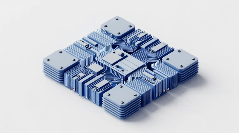
In high-volume digital thermometer production, panelization is not merely a method of arranging boards; it is a critical engineering decision that dictates the velocity of the SMT assembly line. By transitioning from standard rectangular arrays to high-density, multi-up configurations, manufacturers can drastically reduce material scrap rates and improve machine cycle times per unit.
Optimizing Panel Geometry for SMT Throughput
The primary goal of panel optimization is to maintain a constant flow through the pick-and-place machines. By using 'rotation-aware' panel designs, where components are placed in orientations that minimize nozzle movement, manufacturers can shave seconds off every panel cycle, resulting in significant capacity gains over a 24-hour production window.
| Panel Strategy | Material Waste Impact | Throughput Efficiency | Best Use Case |
|---|---|---|---|
| Standard Grid | Moderate (15-20%) | Baseline | Low-volume runs |
| Nested/Staggered | Minimal (<8%) | High | High-volume sensors |
| Strip Panelization | High (>25%) | Very High | Mass-scale, low complexity |
Strategic Considerations for Panel Design
- How does panel density affect tool wear?
While high density increases throughput, it requires more precise V-scoring or routing. Over-dense panels can lead to board warping, potentially increasing defect rates and rework costs. - Why is board fiducial placement critical?
As panel size increases, thermal expansion becomes a factor. Global and local fiducials must be strategically placed to ensure the SMT camera systems maintain alignment accuracy across the entire panel surface. - What role does panel material play?
Choosing standard panel sizes that align with PCB fabricator capabilities avoids premium pricing for custom laminates, directly maximizing ROI.
Implementation Recommendations
To achieve maximum ROI, engineers should adopt a 'Design for Panelization' approach early in the prototyping phase. This includes utilizing software simulations to predict scrap rates and optimizing board layout to ensure that no single component exceeds the stencil capabilities or pick-and-place tool speed limitations.
Minimizing Rework: Addressing Thermal and Mechanical Stresses
Managing Thermal Gradients and Mechanical Fatigue
Thermal management is the cornerstone of high-yield PCBA manufacturing. During reflow, digital thermometers with heterogeneous component footprints—ranging from micro-sensors to large battery contacts—experience significant thermal gradients. These temperature differentials often manifest as warping, solder balling, or component tilting, all of which necessitate costly rework. By utilizing Finite Element Analysis (FEA) to simulate thermal expansion, manufacturers can predict hotspots and adjust solder mask expansion or copper balancing to ensure uniform thermal dissipation across the panel.
| Stress Type | Common Defect | Preventative Strategy |
|---|---|---|
| Thermal Mismatch | Solder Joint Cracking | Optimized Thermal Profiles |
| Mechanical Warp | Open Circuits/Cold Joints | Strategic Via Shielding |
| Vibrational Stress | Component Desoldering | Underfill Implementation |
Best Practices for Reducing Rework
- How does copper balancing impact stress?
Asymmetric copper distribution causes uneven thermal absorption. Implementing copper flooding on signal layers ensures uniform heat transfer, preventing the board from twisting under high temperatures. - Can simulation predict solder joint failures?
Yes. Advanced solder joint reliability modeling allows engineers to stress-test designs virtually before the first prototype is manufactured, highlighting potential fatigue points in the housing/sensor interface. - Is reflow profile tuning effective for mass production?
Standardizing reflow profiles to the specific thermal mass of the thermometer's board ensures that sensitive thermistor sensors are not degraded during the soldering process, significantly reducing scrap rates.
Ultimately, the transition from reactive rework to proactive design-for-manufacturing (DFM) significantly improves ROI. By identifying mechanical stress concentrations early in the CAD phase, we eliminate the root causes of failure rather than simply addressing symptoms on the production line.
The ROI of Automated Optical Inspection (AOI) Integration

The integration of Automated Optical Inspection (AOI) in PCBA production is often viewed as a capital expenditure hurdle; however, when scaling digital thermometer production, it serves as a critical profit-protection mechanism. By catching micro-cracks, solder bridges, and component misalignments at the post-reflow stage, manufacturers eliminate the 'hidden factory' costs associated with shipping defective products to global markets.
Economic Impact: Manual vs. Automated Inspection
| Metric | Manual Inspection | AOI Integration |
|---|---|---|
| Detection Latency | Post-Production | Real-time (In-line) |
| Failure Rate Accuracy | Low (Fatigue-prone) | High (Consistent) |
| Long-term ROI | Negative (Rework/Scrap) | Positive (Yield Gains) |
Key Advantages of AOI in High-Volume Scaling
- Drastic Reduction in Scrap
Identifying solder paste issues immediately after printing prevents the assembly of thousands of faulty PCBs, turning potential scrap into manageable, real-time adjustments. - Scalable Quality Assurance
As production volumes increase, manual inspection becomes an exponential cost variable. AOI scales linearly with throughput without requiring additional labor hours. - Enhanced Data Traceability
AOI systems generate digital audit trails for every unit, providing invaluable data for root-cause analysis in continuous process improvement.
Frequently Asked Questions
- Does AOI increase cycle time?
Modern AOI systems perform inspections in parallel with the assembly cycle, meaning there is negligible impact on the overall line takt time. - Is AOI overkill for simple thermometer boards?
Given the sensitivity of medical-grade thermometers, AOI prevents high-liability field failures that cost orders of magnitude more than the inspection hardware.
Data-Driven Manufacturing: Monitoring Yield Metrics

In the high-volume production of digital thermometers, monitoring yield is not merely a quality control activity; it is a strategic driver of profitability. By systematically tracking First Pass Yield (FPY) and identifying root causes for scrap or rework, manufacturers can shift from reactive maintenance to predictive optimization. This data-driven approach allows for precise calibration of SMT lines and component placement accuracy, directly lowering the cost per unit through decreased material wastage and reduced labor overhead.
Core Metrics for PCBA Yield Optimization
| KPI | Definition | Impact on ROI |
|---|---|---|
| First Pass Yield (FPY) | Percentage of PCBs that pass inspection without rework. | Highest impact; directly reduces production costs. |
| Defects Per Million Opportunities (DPMO) | Frequency of manufacturing defects per million components. | Identifies process instability before major failures occur. |
| Cycle Time Variance | Deviation from expected time per station. | Highlights bottlenecks causing inefficiency and downtime. |
Actionable Insights from Production Data
Data collection must extend beyond the end-of-line testing. Real-time logging of sensor data from reflow ovens, AOI machines, and pick-and-place equipment creates a holistic digital twin of the production line. When a deviation in FPY is observed, correlation analysis can quickly pinpoint if the issue originated from faulty raw materials, machine wear, or atmospheric factors in the cleanroom.
- How does FPY tracking improve long-term ROI?
By maximizing FPY, you minimize costly rework and component loss, ensuring that every raw material purchase is converted into a shippable product efficiently. - What is the role of automated data logging in yield monitoring?
Automated logs eliminate human error and provide a time-stamped history of production variables, which is vital for performing effective root cause analysis during process drift. - When should production processes be re-calibrated based on yield data?
Re-calibration should be triggered when specific KPIs, such as DPMO or FPY, cross pre-defined statistical thresholds, indicating an emerging trend of process instability.
Long-Term Cost of Ownership and Scaling Success
The False Economy of Accelerated Launches
Many manufacturers prioritize speed-to-market by bypassing rigorous DFM protocols, viewing them as obstacles to revenue. However, our case study demonstrates that this 'rapid launch' approach creates a hidden cost burden. When production begins with unoptimized files, the resulting high defect rates and supply chain bottlenecks create a compounding tax on profitability that persists throughout the product lifecycle.
Optimized Production vs. Reactive Troubleshooting
| Category | Reactive/Unoptimized Approach | Strategic DFM Investment |
|---|---|---|
| First Pass Yield | Low (sub-85%) | High (>98%) |
| Rework/Scrap Costs | Excessive | Negligible |
| Scaling Time | Variable/Delayed | Predictable/Fast |
| Long-term TCO | High (maintenance focus) | Low (profitability focus) |
Sustainability Through Scalability
Scaling successful PCBA production for global markets requires transitioning from a 'get it built' mentality to a 'build it optimally' framework. By locking in design efficiencies early, firms avoid the 're-spin' cycle—where engineering changes occur mid-production to fix issues that should have been caught in simulation. This not only protects margins but allows the production line to focus on volume rather than crisis management.
Frequently Asked Questions
- Does DFM investment delay the initial product release?
While front-loading DFM may add a few days to the initial design cycle, it prevents weeks of production downtime and quality-control crises, ultimately leading to a faster market penetration. - How does DFM affect long-term maintenance costs?
DFM-optimized designs are intrinsically more reliable, reducing the frequency of field failures and technical support interventions, which significantly lowers the support cost component of TCO. - At what scale does DFM become cost-effective?
While beneficial at any volume, DFM becomes essential at the high volumes required for digital thermometers, where even a 1% improvement in FPY equates to significant annual savings.
Optimizing your PCBA design is not just a technical requirement—it is a financial imperative for any product scaling to global volumes. By shifting your focus from short-term speed to long-term manufacturing efficiency, you can secure lower unit costs and superior product reliability. Ready to optimize your next production run? Contact our engineering team today to review your DFM strategy and start maximizing your ROI.
