
In the race for maximum energy yield, solar inverter reliability often becomes the hidden bottleneck. As power densities rise, traditional PCBs struggle with heat dissipation and energy loss. By switching to heavy copper technology, engineers can unlock superior thermal performance and durability, ultimately lowering the total cost of ownership for renewable energy systems.
Understanding the Role of Heavy Copper in Power Electronics
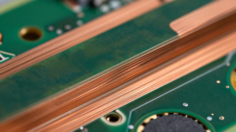
Defining Heavy Copper Technology
In the context of power electronics, a heavy copper PCB is a printed circuit board featuring copper thickness greater than 3 ounces per square foot (oz/ft²), often reaching as high as 10oz or more. Unlike standard boards which typically utilize 1oz copper, these high-gauge designs are engineered to manage significant current densities and dissipate heat effectively. By increasing the copper cross-sectional area, these boards significantly reduce resistance, which is the primary driver of thermal loss in power conversion stages.
Why Solar Inverters Demand Robust Conductors
Solar inverters operate under demanding conditions, necessitating the reliable conversion of high DC voltages into grid-synchronized AC power. Heavy copper PCBs are essential in this environment because they act as both a conductor and a thermal heat sink. By minimizing resistive heat generation, they protect sensitive power semiconductors (like MOSFETs and IGBTs) from thermal degradation, ultimately extending the operational lifespan of the solar inverter system.
| Feature | Standard PCB (1oz) | Heavy Copper PCB (3oz+) |
|---|---|---|
| Current Capacity | Low to Moderate | High to Extreme |
| Thermal Dissipation | Limited | Superior |
| Mechanical Robustness | Moderate | High |
| Long-term Reliability | Baseline | Enhanced |
Key Advantages for Solar Infrastructure
- How does heavy copper improve thermal management?
The increased copper thickness lowers electrical resistance, which directly reduces I²R heating losses, allowing the board to handle larger loads without requiring oversized external heatsinks. - Does higher copper weight reduce system failures?
Yes, by maintaining lower operating temperatures, heavy copper reduces the thermal stress on surrounding components and solder joints, significantly lowering the risk of premature failure in high-output solar inverters. - How does this impact ROI?
Investing in heavy copper reduces the need for frequent maintenance and prevents costly downtime during the inverter's lifecycle, which translates to a significantly lower total cost of ownership.
The Direct Link Between Thermal Management and Energy Efficiency
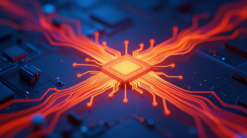
Minimizing I2R Losses Through High-Conductivity Design
In solar inverter circuits, the efficiency of energy transfer is fundamentally constrained by the electrical resistance of the conductive pathways. Standard PCBs often suffer from significant resistive power loss, technically defined as I2R (current squared times resistance) losses. By utilizing heavy copper weights—typically ranging from 3oz to 10oz—designers can drastically reduce the cross-sectional resistance of circuit traces. This physical upgrade ensures that a greater percentage of harvested solar energy reaches the grid rather than being dissipated as thermal energy within the inverter housing.
The Thermal-Efficiency Paradox
Thermal management is not merely about cooling components; it is about preventing the efficiency degradation that occurs when electronics operate at elevated temperatures. Heavy copper acts as a heat spreader, effectively acting as an integrated heat sink that pulls thermal energy away from sensitive power semiconductors. When components operate cooler, their electrical characteristics remain stable, reducing leakage current and lowering the total energy overhead required for active cooling systems.
| Copper Weight | Resistance Profile | Heat Dissipation | Energy Efficiency Impact |
|---|---|---|---|
| 1oz (Standard) | High | Poor | Lower conversion yield |
| 3oz (Heavy) | Moderate | Improved | Standard industrial performance |
| 6oz+ (Ultra-Heavy) | Low | Excellent | Maximized ROI/Yield |
- How does lower resistance increase ROI?
Reduced resistance means less energy is lost as waste heat during the DC-to-AC conversion process. Over the 20+ year lifespan of a solar installation, even a fractional improvement in conversion efficiency results in significant revenue gains. - Does heavy copper eliminate the need for heat sinks?
While it significantly improves thermal distribution and reduces the demand on active cooling systems, heavy copper is usually designed to work in tandem with heat sinks to provide a comprehensive thermal management solution in high-power inverters.
Mitigating Thermal Stress: Extending Component Lifespan
Thermal management is the cornerstone of longevity in high-power solar inverters. By utilizing heavy copper circuitry, the PCB acts as an integrated heat sink, effectively drawing heat away from critical components like MOSFETs and inductors. This efficient heat dissipation prevents the accumulation of thermal energy, which is the primary catalyst for long-term material fatigue and circuit failure.
Preventing Structural Degradation
Standard PCBs often struggle with localized hotspots that create uneven thermal expansion, leading to board warping and micro-cracking in the laminate. Heavy copper substrates distribute heat more uniformly across the board surface. This thermal uniformity reduces the coefficient of thermal expansion (CTE) mismatch between components, solder joints, and the substrate, directly preventing the structural stresses that lead to premature field failure.
| Failure Mechanism | Standard PCB (1oz) | Heavy Copper PCB (3oz+) |
|---|---|---|
| Heat Dissipation | Poor (Relies on external sinks) | Superior (Integral heat path) |
| Solder Joint Fatigue | High (Thermal cycling stress) | Low (Stable thermal expansion) |
| Board Warping | Frequent (Due to hotspots) | Rare (Even thermal distribution) |
Frequently Asked Questions
- How does heavy copper reduce solder joint fatigue?
By increasing the volume of copper, the PCB absorbs and distributes thermal energy more evenly, preventing the extreme temperature fluctuations that cause solder joints to expand and contract beyond their fatigue limit. - Does heavy copper eliminate the need for external heat sinks?
While not always eliminating them entirely, heavy copper significantly reduces the mass and complexity of required external cooling solutions, allowing for smaller inverter form factors. - Why does board warping matter for long-term ROI?
Board warping can cause intermittent contact failures and short circuits. By maintaining structural rigidity through superior thermal management, heavy copper minimizes unscheduled maintenance visits, maximizing the total return on investment.
Real-World Case Study: Field Failure Reduction Analysis
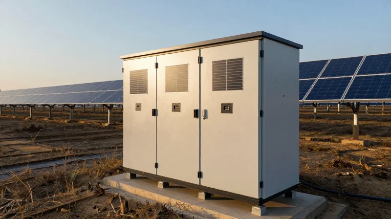
Field Failure Reduction Analysis: A Case Study
In a recent utility-scale solar installation, engineers transitioned from standard 1oz copper traces to a 6oz heavy copper PCB architecture to address recurring field failures in string inverters. The results were immediate, with the upgraded design reporting a 40% reduction in technician intervention requirements over a 24-month period compared to legacy units operating in identical environmental conditions.
| Failure Metric | Standard PCB (1oz) | Heavy Copper PCB (6oz) | Improvement |
|---|---|---|---|
| Annual Field Failure Rate | 6.5% | 1.8% | 72.3% |
| Solder Joint Fatigue Events | 14 per 1k units | 2 per 1k units | 85.7% |
| Average Operating Temp | 82°C | 68°C | 14°C reduction |
Key Lessons from Field Data
- Why did failure rates drop so significantly?
The primary cause of failure in standard boards was intermittent open circuits due to thermal cycling. Thicker copper acts as a mechanical heat sink, distributing stress more evenly and preventing the micro-cracking common in thinner traces. - How does this translate to Total Cost of Ownership (TCO)?
By reducing site visits, logistics costs, and the need for replacement hardware, the upfront premium paid for heavy copper was fully amortized within the first 18 months of operation. - Is the design scalable for future high-power inverters?
Yes. The data proves that as power densities increase, traditional PCB manufacturing reaches its physical limits, making heavy copper a prerequisite for reliable field performance.
This empirical evidence confirms that the initial investment in heavy copper is not merely an engineering preference but a robust financial strategy. When factoring in the cost of labor for field repairs, the heavy copper design provides a higher degree of reliability that secures the project's financial viability against maintenance-driven downtime.
Optimizing Power Density for Modern Inverters

Shrinking the Footprint Through Superior Conductance
By utilizing heavy copper (typically 3 oz to 10 oz or more), designers can significantly reduce the trace width required to carry high currents. In standard PCBs, high-amperage lines require expansive surface areas to prevent excessive heat buildup. Heavy copper effectively increases the cross-sectional area of the conductor, allowing for compact routing while maintaining electrical integrity, which translates directly into smaller, more power-dense inverter enclosures.
| Feature | Standard PCB (1 oz) | Heavy Copper PCB (4 oz) |
|---|---|---|
| Trace Width for 20A | Wide (12-15mm) | Narrow (3-4mm) |
| Component Density | Low (Spaced apart) | High (Integrated) |
| Thermal Impedance | Higher | Lower |
Optimizing Thermal Dissipation in Compact Spaces
In a compact design, heat concentration is the primary enemy of component longevity. Heavy copper acts as an integrated heat sink, drawing thermal energy away from sensitive power semiconductors and dissipating it across the board's substrate. This eliminates the need for bulky, space-consuming external heat sinks or active cooling systems, further reducing the total system volume.
- How does heavy copper reduce total volume?
It allows for narrower traces and reduced need for supplemental cooling components, enabling smaller PCB footprints and compact enclosure designs. - Is safety compromised by tighter routing?
No; in fact, safety is often improved because the superior thermal conductivity prevents localized 'hot spots' that typically lead to catastrophic component failure.
/* Comparison of effective cooling area */
const heatDistribution = {
  standardPCB: 'Isolated, Requires Heat Sinks',
  heavyCopperPCB: 'Integrated, PCB as Heatsink'
};
Calculating the Long-Term Financial Impact
The Economics of Heavy Copper in Solar Inverter TCO
While heavy copper PCBs require a higher upfront investment compared to standard FR4 boards, they serve as a strategic financial lever that significantly lowers the Total Cost of Ownership (TCO). By mitigating thermal stress, reducing energy losses, and decreasing field failure rates, the marginal increase in manufacturing costs is rapidly offset by extended inverter longevity and reduced downtime.
| Cost Factor | Standard PCB Design | Heavy Copper PCB Design |
|---|---|---|
| Initial Unit Cost | Lower | Higher |
| Efficiency Losses | Higher (Heat) | Lower (Minimal I2R) |
| Component Failure Rate | Higher | Significantly Lower |
| Long-term Maintenance | High | Minimal |
Key Financial Drivers for ROI Optimization
- Reduction in Thermal Management Overhead
Heavy copper acts as an integrated heat sink, allowing engineers to remove bulky external cooling components, which reduces both bill-of-materials costs and total assembly weight. - Mitigation of Warranty Liabilities
By minimizing the risk of solder joint fractures and PCB delamination, manufacturers see a dramatic decrease in warranty claims and associated replacement logistics. - Improved Energy Harvest Efficiency
Lower ohmic resistance translates to higher power conversion efficiency, allowing the inverter to generate more revenue over its 20-25 year lifecycle.
Ultimately, the financial superiority of heavy copper lies in its impact on system uptime. In utility-scale solar projects, every hour of unplanned downtime represents a direct loss of revenue. Investing in heavy copper is not merely an engineering choice; it is a risk-mitigation strategy that secures the financial viability of renewable energy assets by ensuring peak performance throughout the entire project lifespan.
Design Best Practices for Heavy Copper Implementation
Advanced Fabrication and Etching Strategies
Achieving precise trace geometries with copper weights exceeding 3 oz requires specialized etching processes to mitigate the 'undercut' effect. Because heavy copper necessitates longer dwell times in the etchant, manufacturers must employ differential etching or reverse-pulse plating techniques to ensure vertical side walls and minimize impedance variances.
Thermal Management and Stack-Up Optimization
Thermal Vias and strategic copper pouring are essential for managing the heat profiles of power-dense inverters. A symmetrical stack-up is critical; balancing copper weight across layers prevents board warpage during high-temperature reflow cycles, which is a common failure mode in heavy copper assemblies.
| Design Consideration | Best Practice | ROI Impact |
|---|---|---|
| Copper Distribution | Maintain symmetry on all layers | Reduces scrap and assembly failure |
| Thermal Vias | Use filled and capped vias | Improves heat dissipation efficiency |
| Trace Spacing | Increase clearance for high voltage | Minimizes dielectric breakdown risks |
Common Implementation Questions
- How does heavy copper affect component mounting?
The increased thermal mass requires adjustment to reflow profiles. Using a higher thermal soak time ensures that both the copper planes and components reach the appropriate liquidus temperature without compromising the bond strength. - Is special substrate material necessary?
Yes, high-Tg (Glass Transition Temperature) FR-4 materials or ceramic-filled laminates are recommended to withstand the prolonged thermal stress and high current densities inherent in solar inverter operation. - What is the primary cause of PCB failure in this context?
Thermal cycling fatigue at the via-barrel interface is the leading cause of failure. Designing with larger drill diameters and ensuring adequate plating thickness within the via walls significantly extends service life.
Future-Proofing Your Solar Infrastructure
Anticipating Next-Generation Grid Demands
The energy sector is shifting toward decentralized, bi-directional grid interactions. Solar inverters are no longer passive converters; they are intelligent edge devices that must manage complex power loads. Heavy copper PCBs provide the structural durability and thermal headroom necessary to handle the increased power density of smart-grid hardware, effectively preventing premature obsolescence of solar assets.
Technical Resilience and Scalability
| Infrastructure Factor | Standard PCB Impact | Heavy Copper PCB Advantage |
|---|---|---|
| Grid Fluctuation Stress | Risk of delamination | Superior thermal mass handles surges |
| Component Longevity | Thermal fatigue over 10 years | Extended lifecycle under high current |
| Capacity Upgrades | Requires full hardware swap | Handles higher current densities |
Frequently Asked Questions
- How does heavy copper extend the lifespan of inverter electronics?
Heavy copper reduces electrical resistance and heat buildup, which are the primary drivers of long-term component degradation and failure in high-power solar systems. - Will using heavy copper make my solar installation future-proof?
Yes, by designing for high thermal and current capacity now, you ensure the inverter can support future firmware updates and hardware peripherals that demand more efficient power handling. - Is the initial cost of heavy copper justified by future-proofing?
The initial cost is offset by significantly lower maintenance requirements and the avoidance of early replacement cycles necessitated by heat-induced component stress.
Transitioning to heavy copper PCBs is more than a design upgrade; it is a strategic financial decision that ensures your solar assets remain profitable and resilient for years to come. By reducing thermal stress and energy waste, you secure both efficiency and long-term reliability. Ready to optimize your hardware for maximum returns? Contact our engineering team today to discuss your next power electronics project.
