In an increasingly complex world, the ability to see beyond the limitations of natural light has become indispensable across various sectors, from defense and security to automotive and wildlife observation. At the heart of every advanced night vision device lies a sophisticated Printed Circuit Board (PCB), dictating its performance, reliability, and precision. Zero One Solution Limited, a leader in rapid-response R&D prototype manufacturing and a comprehensive PCB solution provider since 2011, understands these critical demands. This article delves into how our specialized PCB solutions empower the next generation of night vision technology, ensuring unparalleled clarity and operational excellence in the darkest environments.
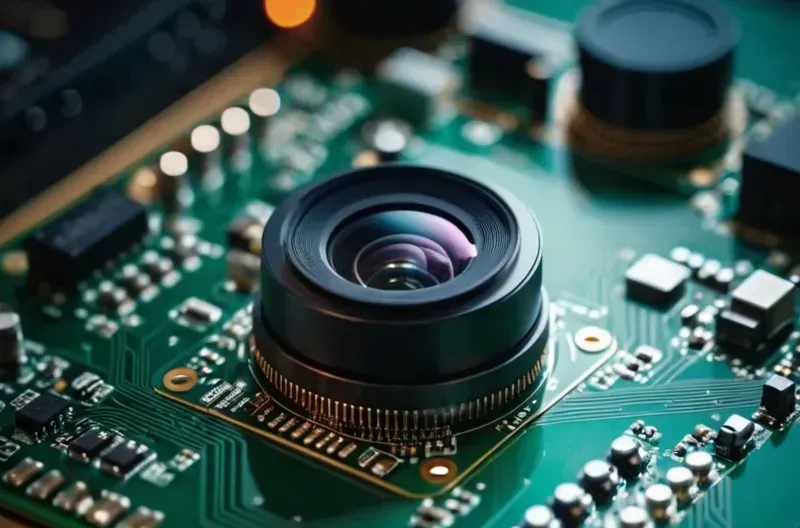
In the demanding realm of night vision technology, the Printed Circuit Board (PCB) is not merely a component; it is the foundational backbone that dictates device performance, image clarity, power efficiency, and overall functionality. A meticulously designed and manufactured PCB is paramount for integrating the complex array of sensors, image intensifiers, power management units, and data processing circuits that define cutting-edge night vision devices, ensuring uncompromised operation in mission-critical scenarios.
| Key Performance Indicator | Impact of PCB | Consequence of Poor PCB Design |
|---|---|---|
| Image Clarity | Precise signal routing, impedance control, and noise reduction directly influence the fidelity and sharpness of the captured image. | Blurry, grainy, or distorted images, compromising target identification and situational awareness. |
| Power Efficiency | Optimized power plane design, low-loss materials, and efficient component placement minimize energy waste. | Shortened battery life, increased heat generation, and reduced operational duration in the field. |
| Signal Integrity | Controlled impedance traces, proper grounding, and crosstalk minimization ensure accurate data transmission. | Signal degradation, data errors, and unreliable performance, especially for high-speed digital and sensitive analog signals. |
class NightVisionPCBSolution {
    // Core requirements for robust night vision PCBs
    public static void main(String[] args) {
        // High signal-to-noise ratio (SNR) for clear imaging
        System.out.println("Requirement: Maximized Signal-to-Noise Ratio (SNR)");

        // Ultra-low power consumption for extended battery life
        System.out.println("Requirement: Minimal Power Consumption");

        // Robustness against extreme environmental conditions (temperature, shock, vibration)
        System.out.println("Requirement: Environmental Durability");

        // Compact footprint for integration into handheld or helmet-mounted devices
        System.out.println("Requirement: Miniaturization");

        // EMI/EMC compliance to prevent interference from internal/external sources
        System.out.println("Requirement: Electromagnetic Compatibility (EMC)");
    }
}Designing Printed Circuit Boards (PCBs) for night vision devices presents a unique confluence of engineering challenges, primarily driven by the need for ultra-sensitive signal processing, extreme miniaturization, and robust performance in harsh operational environments. The intricacies extend beyond standard PCB manufacturing, demanding specialized solutions to overcome hurdles in signal integrity, thermal management, and electromagnetic compatibility. Addressing these complexities is paramount to ensuring the superior image clarity, reliable operation, and prolonged lifespan expected of cutting-edge night vision technology.
| Challenge | Impact on Night Vision Devices | PCB Design Considerations |
|---|---|---|
| Signal Integrity | Compromised image clarity, noise, and data corruption in low-light conditions. | Careful trace routing, impedance control, optimized stack-up, and ground plane design for both analog and high-speed digital signals, minimizing crosstalk and interference. Specific attention to sensitive sensor interfaces. |
| Compact Form Factors & Miniaturization | Limitations on device size, weight, and portability; difficulty integrating complex functionalities. | High-Density Interconnect (HDI) technology, microvias, fine-pitch components, multi-layer designs to maximize component density within constrained spaces. Component selection for smallest footprint. |
| Thermal Management | Overheating of sensitive components (e.g., image intensifiers, IR sensors, FPGAs) leading to performance degradation, reduced lifespan, and potential failure. | Strategic component placement, use of thermal vias, specialized heat-dissipating materials (e.g., metal core PCBs, thermal pads), and efficient power delivery networks to dissipate heat effectively. Simulation and analysis for thermal hotspots. |
| EMI/EMC Shielding | External electromagnetic interference affecting image quality or device functionality; device emissions interfering with other equipment. | Strategic grounding schemes, shielding layers, component isolation, controlled impedance lines, and filtering techniques to minimize electromagnetic interference (EMI) and ensure electromagnetic compatibility (EMC). Proper enclosure design. |
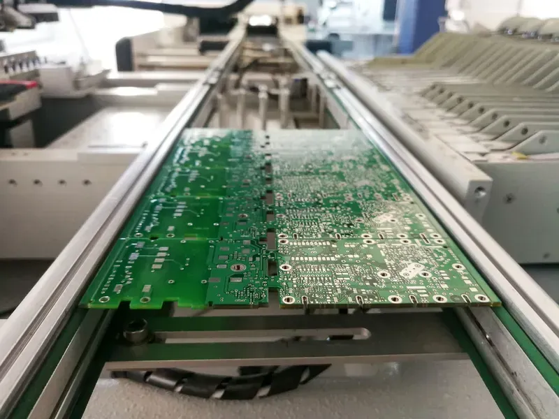
Zero One Solution Limited stands at the forefront of providing specialized PCB solutions for the intricate demands of night vision devices. Our comprehensive capabilities, from rapid prototyping to precision manufacturing, are meticulously tailored to address the unique challenges of military-grade night vision and thermal imaging applications. We empower innovators to accelerate product development by offering a seamless one-stop service from initial design to final assembly, ensuring unparalleled speed, accuracy, and reliability in critical operational environments.
| Capability | Benefit for Night Vision PCBs | Application Examples |
|---|---|---|
| Rapid Prototyping | Accelerated innovation and faster market entry | Early validation of military-grade night vision prototypes |
| Advanced Material Selection | Enhanced signal integrity and thermal management | High-frequency thermal imaging sensor integration |
| HDI Technology | Miniaturization and increased functionality | Compact, high-resolution night vision goggle PCBs |
| Precision Manufacturing | Consistent quality and high reliability | Robust PCBs for demanding field conditions |
| One-Stop Service | Streamlined development and reduced lead times | Seamless transition from design to full-scale production |
Zero One Solution Limited's commitment to excellence extends through every stage of the PCB lifecycle, from initial concept to mass production. Our integrated approach not only simplifies the supply chain for our clients but also guarantees the highest standards of quality and performance for critical night vision device applications. By focusing on precision, speed, and cutting-edge technology, we ensure that our Night Vision Device PCB solutions are built to exceed the stringent demands of this specialized field.

Achieving unparalleled performance in Night Vision Devices hinges critically on the selection of advanced PCB materials and the precision of manufacturing techniques. Zero One Solution Limited leverages cutting-edge materials and sophisticated processes to ensure that every Night Vision Device PCB solution delivers exceptional signal integrity, thermal management, and long-term reliability, even in the most demanding operational environments. This strategic approach to material science and manufacturing engineering is fundamental to transforming theoretical designs into robust, high-performing night vision systems.
| Aspect | Material/Technique | Benefit for Night Vision PCBs |
|---|---|---|
| Substrate Selection | Low-Loss Laminates (e.g., Rogers, Isola) | Minimizes signal attenuation and distortion, crucial for high-frequency signal integrity in imaging circuits and reducing noise in thermal imaging PCB applications. Essential for clearer image transmission and detection range, especially in military-grade night vision devices. These materials offer stable dielectric constants across a wide range of frequencies and temperatures, which is paramount for consistent performance in varying environmental conditions. |
| Impedance Control | Precise Trace Geometry & Dielectric Thickness | Ensures consistent signal propagation and prevents reflections, vital for high-speed digital signals and sensitive analog signals. Critical for maintaining image fidelity and data accuracy in complex night vision systems. Strict impedance control is achieved through advanced design tools and manufacturing processes, guaranteeing that the designed impedance matches the actual impedance on the PCB. This precision is particularly important for high-definition image sensors and integrated communication modules within the device. |
| Multilayer Stack-ups | Optimized Layer Count & Arrangement | Facilitates complex circuit routing in compact spaces, improves power distribution, and enhances EMI shielding. This allows for miniaturization without compromising performance, essential for portable night vision devices. A well-designed stack-up separates noisy digital signals from sensitive analog signals, reducing cross-talk and improving overall system stability. This is crucial for integrating various functionalities, such as image intensification, thermal sensing, and data processing, onto a single, compact board. |
| Surface Finishes | ENIG (Electroless Nickel Immersion Gold) & ENEPIG (Electroless Nickel Electroless Palladium Immersion Gold) | Provides excellent solderability, corrosion resistance, and prolonged shelf life, ensuring reliable component assembly and long-term durability in harsh conditions. These finishes are critical for high-reliability applications where environmental exposure and mechanical stress are concerns, such as military or outdoor night vision equipment. The uniform thickness and flatness of these finishes are also beneficial for fine-pitch component assembly, which is common in miniaturized night vision devices. |
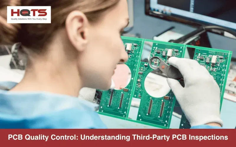
For night vision devices operating in demanding environments, the integrity and reliability of the PCB are paramount. Zero One Solution Limited implements a rigorous, multi-faceted quality assurance framework that extends across every stage of the manufacturing process, ensuring our Night Vision Device PCB Solutions meet the stringent performance and durability requirements of mission-critical applications. Our commitment to excellence is not just about producing functional boards; it's about delivering PCBs that can withstand extreme conditions, maintain signal integrity under stress, and perform flawlessly when lives depend on them.
| Quality Control Stage | Key Methodologies | Benefit for Night Vision Device PCBs |
|---|---|---|
| Design Review & DFM | Rigorous DFM (Design for Manufacturability) analysis, signal integrity simulations, thermal modeling. | Minimizes design flaws, optimizes layout for performance and manufacturability, ensures thermal stability, preventing costly re-spins and enhancing overall reliability from the outset. |
Our commitment extends to adherence to stringent industry standards, including IPC-A-610 (Acceptability of Electronic Assemblies) and IPC-6012 (Qualification and Performance Specification for Rigid Printed Boards). These standards guide our manufacturing processes, material selection, and inspection criteria, ensuring that every Night Vision Device PCB we produce meets global benchmarks for quality and reliability. By integrating these rigorous testing and quality control measures, Zero One Solution Limited guarantees that our PCBs are not just built, but meticulously engineered and verified for the uncompromising demands of mission-critical night vision applications, ensuring exceptional durability and operational performance in the most challenging environments.
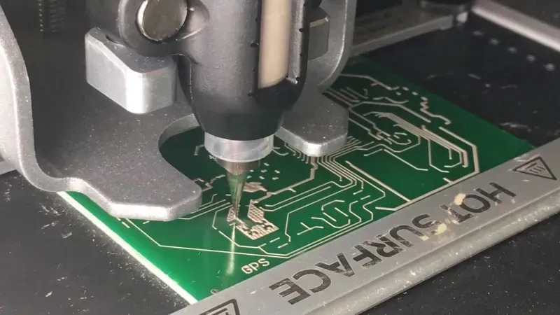
In the fast-evolving landscape of night vision technology, rapid prototyping and extensive customization of Printed Circuit Boards (PCBs) are not just advantages, but necessities. Zero One Solution Limited empowers innovators to significantly compress product development cycles and accelerate the market entry of groundbreaking night vision devices. Our agile manufacturing approach, combined with deep engineering expertise, ensures that unique project specifications for Night Vision Device PCBA are not only met but optimized for performance and reliability.
| Feature | Benefit for Night Vision PCB | Impact on Innovation |
|---|---|---|
| Rapid Prototyping | Quick validation of complex designs, reduced time-to-market. | Accelerated R&D cycles, faster product launches |
| Custom Stack-ups | Optimized signal integrity and impedance control for specific sensors. | Enhanced image clarity and system performance |
| Material Customization | Tailored thermal management and dielectric properties. | Improved device reliability and longevity in diverse environments |
| Flexible Manufacturing | Scalable production from low-volume prototypes to mass production. | Seamless transition from concept to commercialization |
Understanding the intricacies of Printed Circuit Boards (PCBs) for night vision devices is crucial for anyone involved in their development or procurement. This section addresses frequently asked questions, providing clear, concise, and authoritative answers to common inquiries about the design, manufacturing, and specific considerations for Night Vision Device PCB Solutions, ensuring optimal performance and reliability in mission-critical applications.
Zero One Solution Limited stands as your premier partner for Night Vision Device PCB Solutions. Our commitment to rapid prototyping, design excellence, and high-quality manufacturing, combined with our global supply chain network, ensures that your innovative night vision concepts transition from idea to market with unprecedented speed and reliability. By choosing Zero One Solution, you're not just getting a PCB; you're gaining a strategic advantage in a highly competitive landscape, backed by two decades of Silicon Valley expertise and a dedication to pushing the boundaries of what's possible in low-light imaging. Contact us today to discuss how our expertise can illuminate your next project.

