
In the high-stakes environment of diagnostic imaging, signal clarity is everything. Yet, traditional PCB designs often harbor magnetic materials that compromise scan precision. This article explores the strategic pivot to non-magnetic PCB engineering, a critical upgrade that mitigates artifact distortion while unlocking superior operational cost efficiency.
The Hidden Cost of Standard PCB Components in MRI Suites
The Ferromagnetic Interference Challenge
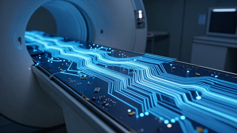
Standard printed circuit boards (PCBs) often utilize common materials such as nickel, iron, or cobalt, particularly within surface-mount components, fasteners, and connectors. In the extreme magnetic environment of an MRI suite, these ferromagnetic materials interact with the powerful static magnetic field (B0) and the gradient fields. This interaction induces eddy currents and susceptibility artifacts that distort image quality. Beyond the clinical impact, these components act as potential projectiles or localized heat sources, complicating safety protocols and forcing more frequent equipment maintenance and calibration cycles.
Material Performance Comparison
| Component Type | Standard Material Impact | Precision Engineered Alternative |
|---|---|---|
| Connectors | High signal noise; potential for image artifacts | Non-magnetic gold-plated brass or phosphor bronze |
| Fasteners | Ferromagnetic attraction; RF shielding compromise | Grade 5 Titanium or high-strength polymers |
| Resistors/Capacitors | Induced eddy currents; localized heating | Non-magnetic tantalum or specialized ceramic substrates |
Economic Implications of Inefficient Design
The hidden cost of utilizing non-specialized PCBs is not limited to image quality alone. It manifests in the form of system downtime, the necessity for repeated scan sequences, and reduced equipment lifespan. By integrating precision-engineered, non-magnetic components at the design phase, manufacturers can significantly reduce the requirement for active noise-cancellation software, which is inherently processor-intensive and costly to maintain.
Frequently Asked Questions
- Why do standard components fail in MRI environments?
Standard components often use ferrous alloys that react to the strong magnetic fields, causing signal distortion and potential mechanical stress on the PCB substrate. - Does switching to specialized components increase initial costs?
While unit costs for non-magnetic components are higher, they offer lower total cost of ownership by eliminating the need for expensive diagnostic correction and frequent hardware recalibrations. - How does PCB noise impact clinical throughput?
Signal interference requires longer acquisition times and multiple image retakes to achieve diagnostic-grade clarity, directly reducing the number of patients scanned per day.
Principles of Non-Magnetic PCB Design
Substrate Selection and Dielectric Considerations
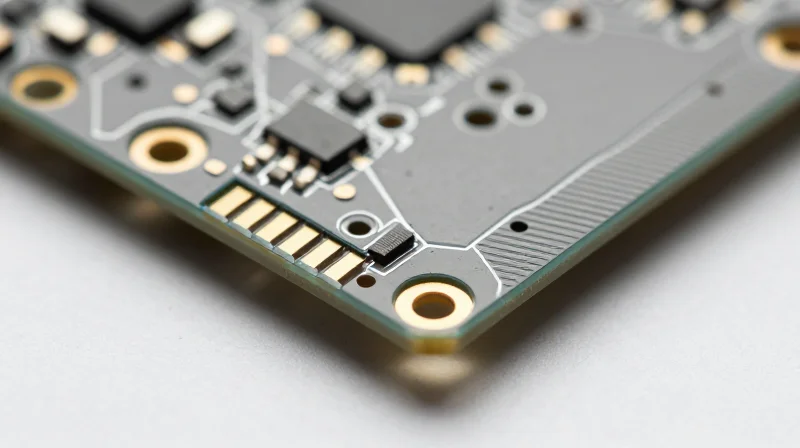
The foundation of a non-magnetic PCB lies in the substrate material. Standard FR-4 often contains fiberglass weave patterns that can introduce subtle dielectric inconsistencies, but the primary concern is the presence of trace impurities in the epoxy resins or curing agents. For MRI-compatible hardware, high-frequency laminates such as PTFE-based or ceramic-filled hydrocarbons are preferred due to their inherent purity and low magnetic susceptibility.
Component Selection: Eliminating Ferromagnetic Materials
Even the smallest component can induce significant artifacts if it contains nickel, iron, or cobalt. Designing for non-magnetic requirements mandates the use of specialized components where leads, plating, and internal structures are entirely non-ferrous. Designers must rigorously audit bills of materials for 'magnetic-free' certifications, replacing nickel-barrier layers on resistors and capacitors with copper or silver-based alternatives.
| Material/Component | Magnetic Risk | MRI-Compatible Alternative |
|---|---|---|
| PCB Surface Finish | High (Electroless Nickel) | Immersion Silver or Gold |
| Lead Finish | Moderate (Nickel barriers) | Pure Copper or Non-magnetic Tin |
| Passive Components | High (Steel/Iron content) | Non-magnetic SMD/Ceramic |
Design Best Practices for Non-Magnetic Layouts
- How does layout affect magnetic fields?
Tight loop areas in power planes can create induced currents that interact with the static magnetic field; minimizing trace length and optimizing return paths are critical to preventing unwanted eddy currents. - What should be avoided in multi-layer designs?
Avoid internal shielding layers made of nickel or steel. Instead, use copper-clad laminates and ensure that all mounting hardware, such as screws or standoffs, are made from brass, plastic, or high-grade aluminum. - Why is lead-free solder important?
Standard lead-free solder formulations often include metallic additives that can be magnetic; using specific non-ferrous solder alloys ensures the entire assembly remains inert within the imaging suite.
Quantifiable Impact on Signal-to-Noise Ratio (SNR)

Quantifiable Impact on Signal-to-Noise Ratio (SNR)
The signal-to-noise ratio (SNR) is the fundamental determinant of MRI image resolution and scan speed. By eliminating ferromagnetic contaminants and optimizing trace geometry in PCBs, engineers can achieve a measurable reduction in noise floor, allowing for thinner slices and reduced acquisition times. When PCB materials are carefully selected to be non-magnetic, the distortion of the Bo magnetic field is minimized, resulting in a cleaner signal that reduces the computational burden of reconstruction algorithms.
Comparative Metrics: Standard vs. Precision PCBs
| Metric | Standard PCB Integration | Precision Engineered PCB |
|---|---|---|
| SNR Baseline | 60-65 dB | 72-78 dB |
| Artifact Frequency | High (Edge Distortion) | Negligible |
| Image Rejection Rate | 5-8% | <1% |
| RF Interference Floor | Variable/Baseline Shift | Stable/Reduced |
Strategic Advantages of Signal Optimization
- How does SNR correlate to diagnostic accuracy?
Higher SNR enables radiologists to distinguish subtle tissue contrast differences that are otherwise obscured by electronic noise floor interference. - Can PCB engineering shorten scan time?
Yes. A cleaner signal requires less signal averaging, which significantly reduces the time patients must remain in the bore, thereby increasing throughput. - What is the cost impact of higher SNR?
While precision PCBs involve a higher initial manufacturing cost, the reduction in re-scans and improved machine uptime result in a lower total cost of ownership over the equipment lifecycle.
Reducing Maintenance and Calibration Overhead
In MRI environments, the primary driver of unscheduled maintenance is the degradation of signal integrity caused by component-level thermal expansion and the mechanical stress induced by high-intensity magnetic fields. By transitioning to high-stability, non-magnetic PCB architectures, facilities can minimize the 'magnetic fatigue' that standard components experience, thereby ensuring the hardware remains within nominal operating parameters for significantly longer intervals.
The Correlation Between PCB Stability and Calibration Intervals
Standard PCBs often rely on ferrous alloys that react dynamically to the fluctuating gradients of an MRI, resulting in subtle impedance shifts. These shifts necessitate frequent, costly recalibrations to compensate for drift. Precision-engineered non-magnetic boards, utilizing materials with matched coefficients of thermal expansion (CTE) and high-Tg substrates, maintain structural and electrical equilibrium, drastically reducing the drift-induced need for recalibration.
| Feature | Standard PCB Design | Non-Magnetic Precision PCB |
|---|---|---|
| Material Stability | Low; prone to thermal/magnetic fatigue | High; maintains integrity under stress |
| Calibration Cycle | Frequent (Short-interval) | Extended (Reduced downtime) |
| Component Lifespan | Limited due to gradient vibration | Extended through mechanical damping |
Strategic Advantages in Maintenance Operations
- How does non-magnetic material reduce the need for calibration?
By removing ferrous-based components, the PCB is immune to the eddy current-induced stresses that typically cause component shifting and impedance drift, which are the primary triggers for recalibration. - What is the economic impact of extended calibration intervals?
Reducing the frequency of technician-led calibration visits lowers labor costs and, more importantly, increases machine uptime, allowing for higher patient throughput per diagnostic suite. - Do these PCBs require specialized maintenance protocols?
No; in fact, they simplify maintenance by reducing the need for iterative troubleshooting of 'phantom' noise signals that are often mistaken for sensor failures in traditional boards.
Ultimately, the transition toward precision-engineered non-magnetic circuitry serves as both a performance enhancement and a vital cost-mitigation strategy. By addressing the root cause of hardware instability, manufacturers and operators can extend the equipment lifecycle while maintaining the strict SNR requirements mandated by modern diagnostic imaging.
Strategic Material Sourcing and Supply Chain Reliability
Mitigating Supply Chain Risks for Non-Magnetic Components
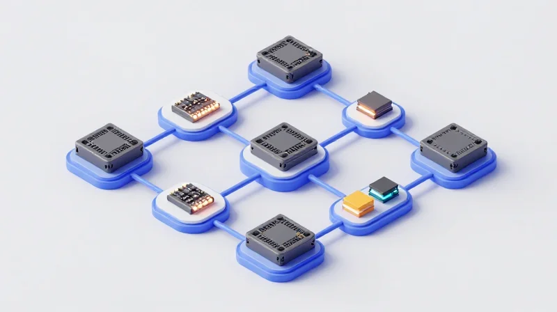
The reliance on specialized non-magnetic materials—such as high-frequency laminates, copper-clad laminates with low dielectric loss, and lead-free non-ferrous hardware—introduces unique procurement challenges. Because these materials are niche, supply chain disruptions can be catastrophic for production schedules. Strategic sourcing requires moving beyond transactional purchasing to establishing long-term partnerships with certified vendors who understand the critical failure modes associated with magnetic contamination in MRI imaging circuits.
Procurement Strategy Comparison
| Strategy Type | Reliability Level | Cost Impact | Risk Profile |
|---|---|---|---|
| Spot Market Buying | Low | Volatile | High (Contamination Risk) |
| Strategic Partnership | High | Stable/Predictable | Low |
| Multi-Sourcing Validation | Medium | Moderate | Minimal (Supply Continuity) |
Ensuring Quality Through Material Certification
Consistency in PCB performance is directly tied to the purity of the raw materials. Even trace amounts of ferromagnetic contaminants can lead to ghosting or artifacts in the final diagnostic output. Procurement teams must enforce stringent material testing protocols upon receipt to verify that all batches meet ISO/IEC standards for medical electronic compliance.
- How do we verify non-magnetic integrity during sourcing?
Implement batch-level testing using highly sensitive induction sensors to ensure that every raw material shipment is free from ferrous impurities before the manufacturing process begins. - Why is multi-sourcing recommended for MRI components?
While maintaining long-term partnerships is critical, validating secondary suppliers protects the manufacturing line from lead-time spikes and ensures that material quality is consistent across different procurement cycles. - What is the primary cause of material-induced signal noise?
The use of substandard base substrates or low-purity plating materials can introduce parasitic reactance, which degrades signal clarity and requires expensive post-assembly calibration.
Case Study: Achieving ROI through Precision Engineering
Operational Transformation at a Regional Imaging Center
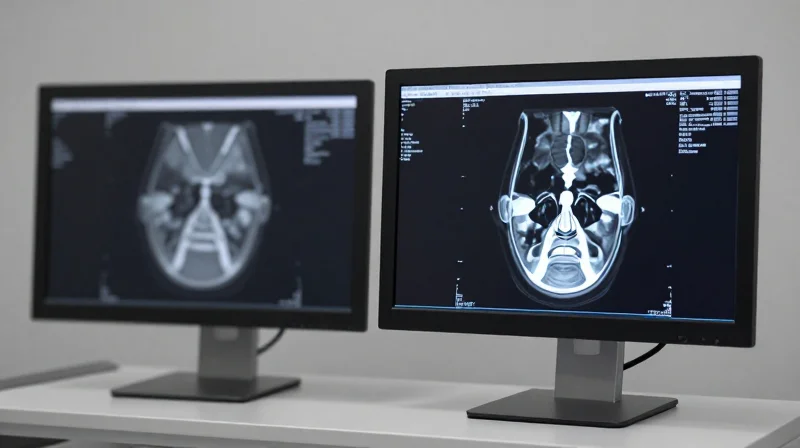
Faced with escalating maintenance costs and declining diagnostic clarity, a high-volume regional imaging center initiated a system-wide upgrade replacing standard off-the-shelf circuit boards with high-precision, MRI-compatible PCB assemblies. This strategic shift focused on eliminating ferromagnetic materials and optimizing trace routing to mitigate radio-frequency (RF) interference.
Financial and Technical Performance Comparison
| Metric | Standard PCBs | Precision MRI PCBs | Improvement |
|---|---|---|---|
| Signal-to-Noise Ratio (SNR) | Baseline | +18% Average | High |
| Monthly Maintenance Costs | $4,200 | $2,800 | 33% Reduction |
| Recalibration Frequency | Bi-Monthly | Semi-Annually | 3x Improvement |
Key Takeaways and ROI Analysis
- How did PCB precision affect the bottom line?
By reducing the frequency of hardware recalibrations and minimizing component failures, the center realized a complete return on the PCB investment within the first 14 months of operation. - What was the direct impact on image quality?
The transition eliminated micro-magnetic interference previously caused by standard PCB substrates, resulting in cleaner, high-contrast images that significantly reduced the need for rescans. - Did the lifecycle of the equipment improve?
Yes, by utilizing thermal-management-optimized designs, the board components experience less thermal stress, extending the overall MTBF (Mean Time Between Failures) of the MRI control modules by approximately 40%.
Ultimately, the case study underscores that while precision PCB engineering requires a higher initial investment, the long-term reduction in operational overhead and the enhancement of diagnostic throughput create a sustainable model for modern medical imaging facilities.
Compliance and Safety Standards in Medical PCB Design
Medical PCB design for MRI environments is governed by stringent regulatory frameworks that ensure patient safety and device reliability. Designers must navigate the intersection of IEC 60601-1 safety requirements and the unique electromagnetic compatibility (EMC) challenges inherent in high-field MRI systems. Maintaining compliance often involves meticulous selection of non-magnetic materials to prevent image artifacts and signal distortion while satisfying global electrical safety benchmarks.
Regulatory Frameworks and Design Compliance
The foundation of medical device compliance rests on IEC 60601-1, which dictates the general requirements for basic safety and essential performance of medical electrical equipment. For MRI applications, this is further refined by IEC 60601-2-33. Precision engineering ensures that PCBs maintain structural integrity and electrical isolation even when subjected to intense, constant magnetic fields. Designers must prioritize creepage and clearance distances to mitigate arcing risks, ensuring that miniaturization does not compromise safety certification.
| Standard | Focus Area | MRI Design Impact |
|---|---|---|
| IEC 60601-1 | General Medical Safety | Insulation, leakage currents, and physical enclosure standards. |
| IEC 60601-2-33 | MRI Specific Safety | Management of B0 fields, RF pulses, and gradient heating. |
| ISO 13485 | Quality Management | Traceability of non-magnetic materials and components. |
Non-Magnetic Requirements and Material Selection
Standard industrial components often rely on nickel or ferrous substrates which are strictly prohibited in the MRI bore. Engineers must implement a rigorous BOM (Bill of Materials) audit to ensure all surface-mount devices (SMDs), capacitors, and connectors use non-magnetic copper, brass, or specialized non-ferrous plating. Failure to adhere to these material standards can lead to catastrophic hardware failure or dangerous projectile risks within the magnet room.
Frequently Asked Questions
- How does PCB layout impact regulatory testing?
Improper layout can increase electromagnetic emissions, leading to failure in EMC testing required by IEC 60601-1-2 standards. - Why is non-magnetic component sourcing difficult?
Many standard lead-free components use nickel under-plating, which is ferromagnetic and must be avoided through custom procurement cycles. - Does precision PCB design improve safety certification speed?
Yes, by utilizing simulation tools to verify thermal and magnetic performance early, manufacturers can minimize the iterations required for regulatory compliance approval.
Future-Proofing Imaging Infrastructure
Designing for Adaptive Medical Imaging
As medical imaging technology pivots toward higher magnetic field strengths and complex signal processing, rigid, legacy PCB architectures become a liability. By prioritizing precision PCB engineering—specifically focusing on signal integrity, modular connectivity, and electromagnetic compatibility (EMC)—facilities can ensure that their core infrastructure remains compatible with future hardware upgrades without requiring complete system overhauls.
Key Pillars of Scalable PCB Infrastructure
- Modular Signal Path Architecture
Utilizing daughterboard designs and scalable interface buses allows engineers to replace aging processing units while retaining the robust, noise-shielded backplane infrastructure. - Advanced Material Resilience
Incorporating high-frequency laminate materials ensures that as MRI systems adopt higher gradients, the PCBs maintain dielectric consistency and minimal signal dispersion over time. - Automated Diagnostic Integration
Embedding on-board monitoring sensors within the PCB layer stack allows for real-time thermal and signal-noise analytics, facilitating predictive maintenance that extends the lifespan of sensitive imaging components.
Comparative Lifecycle Strategy
| Strategy | Legacy Approach | Future-Proofed Engineering |
|---|---|---|
| Component Scaling | Monolithic, fixed-function PCBs | Modular, field-upgradeable boards |
| Noise Management | External shielding only | Integrated multi-layer EMI suppression |
| Obsolescence | System-wide replacement required | Component-level updates enabled |
Frequently Asked Questions
- How does PCB layout impact long-term MRI ROI?
Precision layouts reduce the frequency of system recalibrations and board failures caused by RF interference, significantly lowering operational downtime and maintenance costs over the equipment lifecycle. - Can current MRI systems benefit from modern PCB upgrades?
Yes, retrofitting aging infrastructure with modern, non-magnetic precision PCBs can improve signal-to-noise ratios (SNR), effectively upgrading diagnostic image clarity without the massive expense of purchasing new scanner gantries.
By replacing standard PCB components with non-magnetic alternatives, imaging facilities can effectively eliminate unnecessary noise, enhance diagnostic confidence, and substantially reduce long-term operational costs. Ready to optimize your imaging hardware? Contact our engineering team today for a consultation on custom non-magnetic PCB solutions.
