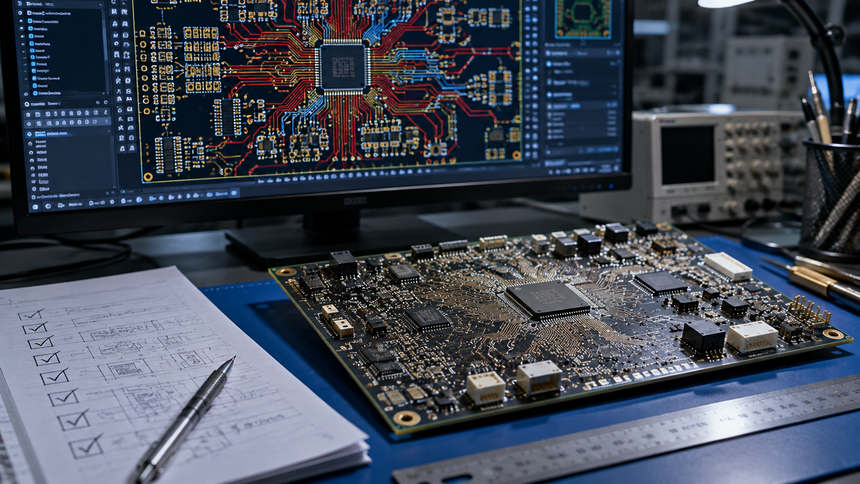
Whether you're working on a high-speed design or a conventional PCB, good board-level design practices help ensure your design performs as intended and can be manufactured at scale. This guide covers the core PCB design layout principles that apply to most modern circuit boards — from design rule setup and component placement to routing strategies and manufacturing output.
When starting a new PCB design, it's easy to forget to set up critical design rules. Simple spacing requirements, if defined early, can prevent extensive component movement and rerouting later in the design cycle.
Start by communicating with your PCB manufacturer. A good manufacturer typically publishes their manufacturing capabilities online. It's best to do this before you begin placing components. Also, submit your proposed stackup for review, or use the manufacturer's standard stackup data.
Once you have the manufacturer's capability list, compare these capabilities against any industry reliability standards you need to follow. After identifying these requirements, you should choose more conservative design constraints to ensure manufacturability and reliability, and apply these constraints to your PCB design rules.
Throughout the layout process, your PCB design rules will help eliminate most design errors that could cause manufacturing or assembly issues. Once board-level design rules are set, you can begin the layout process.
Component placement is both an art and a science, requiring strategic use of the available board area. The goal is to create a board that's easy to route, ideally minimizing layer transitions, while meeting all design rules and component placement requirements.
1. Place required components first. Some components must be placed in specific positions due to mechanical enclosure constraints or size requirements. Place these first and lock their positions before proceeding.
2. Place large processors and ICs. High-pin-count ICs or processors typically need to connect to multiple components. Placing these centrally makes routing easier.
3. Minimize net crossings. When components are placed, you can often see unrouted nets. Try to minimize the number of net crossings. Each crossing requires a via for layer transition. Creative placement can eliminate crossings and simplify routing.
4. SMD placement guidelines. Place all surface-mount components on the same side of the board when possible. This is primarily for assembly reasons — each side requires separate SMT line passes, so placing all SMDs on one side helps avoid additional assembly costs.
5. Adjust orientation. Rotate components to try to eliminate net crossings. Align connected pads to face each other — this simplifies routing.
Following these steps makes routing the rest of the board much easier. Your board will have a modern layout appearance — a central processor delivering data to all other components around the board.
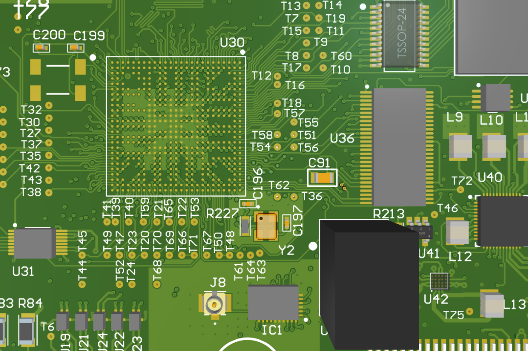
After completing component placement, route power, ground, and signal traces to ensure clean, interference-free signal paths.
It's generally recommended to place power and ground planes on two inner layers. For 2-layer boards, this is harder to achieve, so it's better to place a large ground plane on one layer and route signals and power on the other.
For 4-layer or higher stackups, use ground planes instead of ground traces. For components requiring direct power connections without a dedicated power plane, use a common bus for each power system — use sufficiently wide traces (100 mil traces can handle 5-10A) and avoid daisy-chaining power between components.
Some guidelines require symmetrical plane arrangements, but this isn't a manufacturing requirement. On large boards, symmetrical placement helps reduce warpage beyond EMI considerations, but is less critical for small boards. Prioritize power and ground accessibility, and ensure all traces have strong return path coupling to the nearest ground plane.
Place short, direct traces between components whenever possible, though this may not always be feasible on larger boards. If component placement forces horizontal routing on one side, always route vertically on the other — this is a key rule for 2-layer board design.
As layer count increases, routing rules become more complex. Your routing strategy should alternate horizontal and vertical routing on alternating layers, unless you separate each signal layer with reference planes.
Trace width depends on three factors:
| Factor | Description |
|---|---|
| Manufacturability | Traces can't be too thin to be reliably manufactured. In most cases, your trace width will be far wider than the manufacturer's minimum. |
| Current | Trace current determines the minimum width needed to prevent overheating. Higher currents require wider traces. |
| Impedance | High-speed digital or RF signals require specific trace widths to achieve required impedance. This doesn't apply to all signals or nets. |
For traces not requiring specific impedance or carrying high current, 10 mil trace width is sufficient for most low-current analog and digital signals. Traces carrying more than 0.3A may need to be wider. Use IPC-2152 nomographs to determine trace width meeting current capacity and temperature rise requirements.
Ground planes act as large heatsinks, spreading heat evenly across the board. When connecting through-hole components to ground planes, omitting thermal relief allows heat to conduct into the ground plane — better thermal management than keeping heat on the surface.
However, if through-hole components are wave-soldered, this creates issues because the process requires heat concentration on the surface. Thermal relief pads ensure through-hole solder joints are manufacturable in wave soldering by slowing heat conduction into the plane, preventing cold solder joints.
Through-hole pads on copper pours may require thermal relief similar to planes. When copper pours are large, they behave like planes, so thermal relief should be applied.
For surface-mount (SMD) components, the situation is different. During reflow soldering, the entire board heats uniformly, so SMD pads with or without thermal relief have much lower tombstoning risk than with other soldering methods.
For hand-assembled designs using paste and hot-air guns, thermal relief connections may be needed to maintain enough heat near pads and prevent tombstoning.
Design rules for grouping and isolating components and traces ensure easy routing while preventing electrical interference. These grouping guidelines also aid thermal management.
Break circuits into functional sections. Each section only connects to specific circuits, so you don't need to place components on different sides or areas. PCB layout becomes the process of designing and placing individual circuit groups so they can be easily connected by traces.
Many boards contain both analog and digital components — you must prevent digital components from interfering with analog components.
Correct practice: Use a complete ground plane under components and avoid physically splitting ground planes. Group analog components operating at the same frequency together, and group digital components similarly. Components should be zoned above the ground plane, but the ground plane should remain whole in most designs.
Spread high-heat components across different areas to balance temperature across the board, rather than creating hot spots. Use heatsinks and cooling fans to reduce temperatures. You may need to carefully balance high-power component placement with keeping trace lengths short.
Near the end of your project, checking your work for errors can mean the difference between manufacturing success and failure.
Start with Electrical Rule Check (ERC) and Design Rule Check (DRC) to verify you meet all established constraints. These systems let you define clearances, trace widths, manufacturing constraints, high-speed electrical requirements, and other physical requirements.
Many design flows recommend running DRC at the end of the design phase, before manufacturing preparation. With proper design software, you can run checks throughout the design process, allowing early detection and correction of potential issues.
When your final ERC and DRC produce error-free results, review each signal's routing and check against the schematic — trace by trace — to confirm nothing is missing.
These PCB layout core principles apply to most circuit board designs. From design rule setup and component placement to routing strategies and manufacturing output, each step requires careful planning and execution.
Key principles recap:
Define manufacturing rules and stackup early in the design phase
Place critical components first, then position the rest
Use planes for power and ground rather than traces
Maintain complete ground planes — avoid physical splits
Run DRC throughout the design phase to catch issues early
Consider thermal relief pads and thermal management needs
Need PCB Design Support?
AnyPCBA's engineering team focuses on component placement, power integrity, signal integrity, and manufacturability during design reviews. Whether you're working on prototype verification or production preparation, we provide DFM/DFA design reviews to identify potential risks in layout, routing, and stackup before fabrication.
Our manufacturing capabilities cover 2-64 layers, including HDI, rigid-flex, and high-frequency hybrid processes.
Contact us to discuss your project →




