In the intricate dance of modern electronics, the PCB stencil plays a pivotal role, akin to a master key unlocking precision in surface mount technology (SMT) assembly. Like an artist using a carefully crafted mold, a PCB stencil maker creates the tool that ensures consistent solder paste application onto printed circuit boards. This article dives deep into the world of PCB stencils, exploring their types, manufacturing, and how they impact the efficiency and quality of electronic device production. From understanding materials to selecting the best stencil for your project, we will navigate the essential aspects to empower you with the knowledge of a PCB stencil maker.
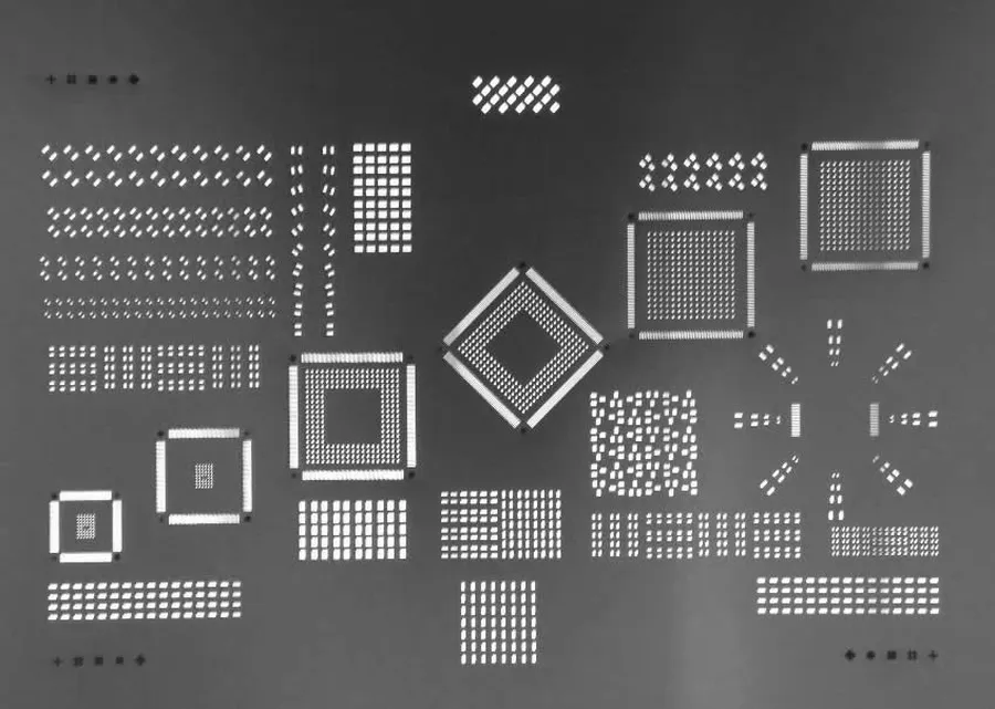
PCB stencils are fundamental tools in Surface Mount Technology (SMT) assembly, ensuring precise solder paste deposition onto printed circuit boards. This accuracy is paramount for creating reliable electronic devices, as it dictates the quality of electrical connections between components and the board.
The stencil acts as a template, guiding the solder paste application process by allowing it to be deposited only in the required locations, thus ensuring correct placement on component pads. Inaccurate deposition leads to defects, such as shorts, opens, and insufficient solder joints, which can compromise the performance of the circuit or cause device failure. This critical first step in the SMT process directly impacts the final product's overall reliability and performance.
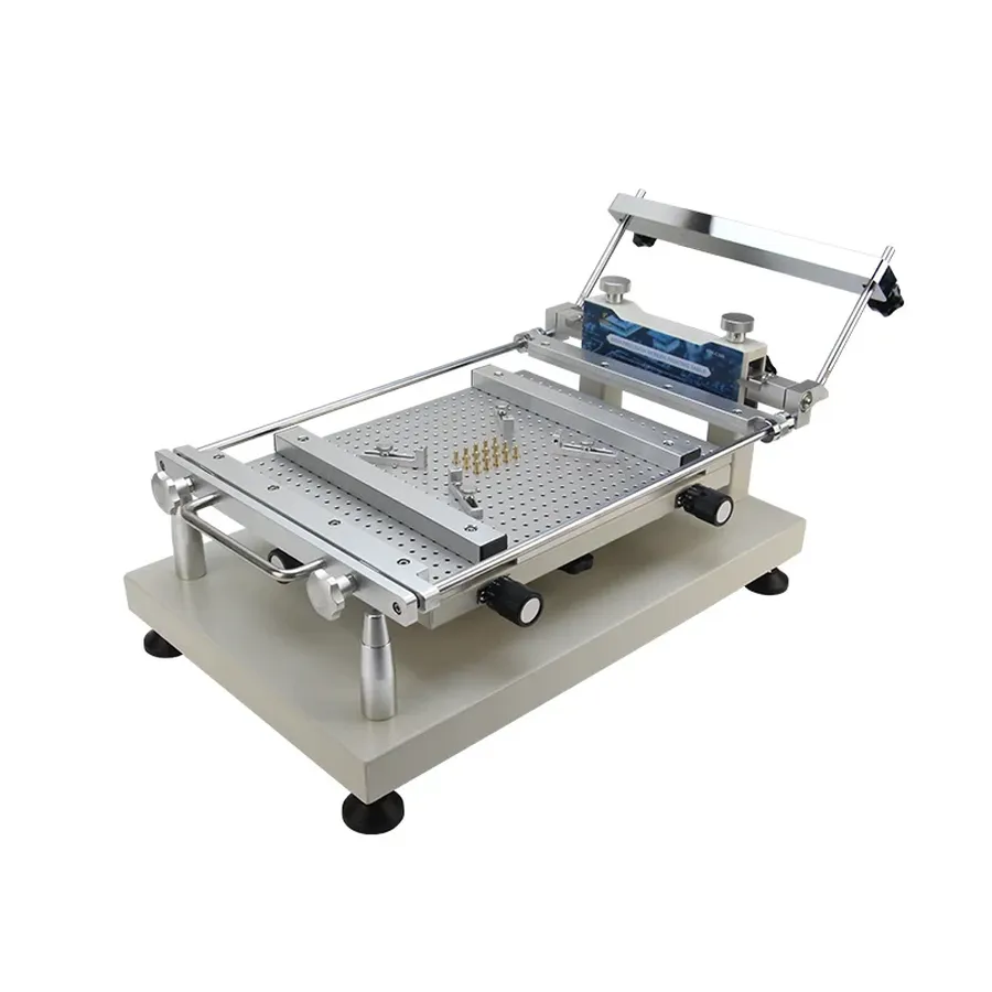
PCB stencils are essential tools in surface mount technology (SMT) assembly, facilitating the precise application of solder paste onto circuit boards. These stencils come in three primary types: framed, frameless, and prototype, each designed for specific production needs and offering distinct advantages and limitations.
| Stencil Type | Description | Advantages | Disadvantages | Typical Application |
|---|---|---|---|---|
| Framed Stencil | A stencil permanently mounted in a frame. | High durability, excellent for high-volume production, precise alignment, easy to handle. | Higher cost, requires storage space, less flexible for modifications. | High-volume SMT assembly, automated production lines. |
| Frameless Stencil | A stencil sheet that is tensioned in a frame when in use. | Cost-effective, requires less storage space, flexible for adjustments. | Less durable than framed stencils, requires a tensioning system, can be challenging for automated processes. | Medium-volume production, where flexibility and cost efficiency are important. |
| Prototype Stencil | Typically smaller, lower cost stencils for initial testing. | Very cost-effective for small quantities, good for quick prototyping, allows design iteration. | Less durable, not suited for high-volume production, may have lower precision. | Low-volume prototyping, small-scale production, testing of new designs. |
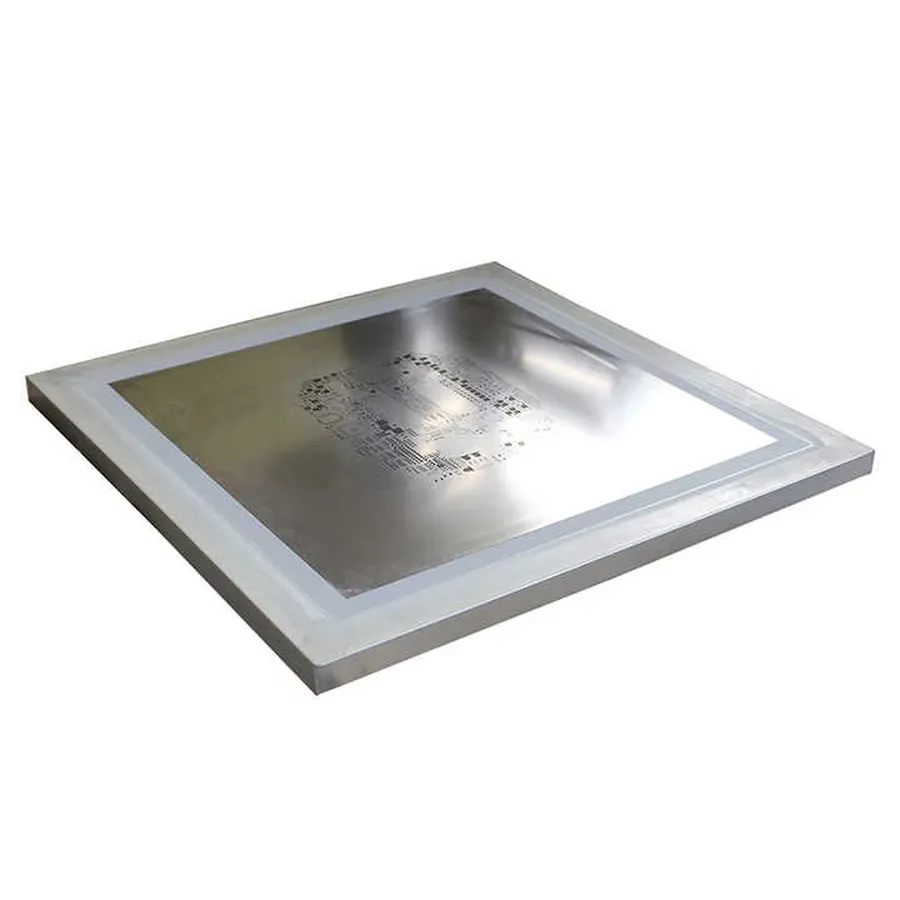
The selection of materials for PCB stencils is crucial, directly impacting stencil performance, durability, and cost. Two primary materials dominate the industry: stainless steel and polyimide (Kapton). Each offers a unique set of characteristics that make them suitable for different applications and production volumes.
| Material | Properties | Typical Application | Advantages | Disadvantages |
|---|---|---|---|---|
| Stainless Steel | High strength, durable, excellent dimensional stability, chemically inert. | High-volume production, fine-pitch components, reusable stencils. | Long lifespan, precise aperture definition, suitable for frequent use, resists wear and tear. | Higher cost, not as flexible as polyimide. |
| Polyimide (Kapton) | Flexible, lightweight, moderate dimensional stability, good chemical resistance. | Prototype runs, low-volume production, stencils with intricate designs and tighter tolerances. | Cost-effective for small runs, can be more precise for certain designs, flexible for uneven boards. | Lower durability, not suitable for high-volume use, can stretch or deform over time, shorter lifespan, less precise for large apertures. |
Stainless steel stencils are preferred for high-volume manufacturing due to their robustness and ability to withstand frequent use without compromising accuracy. Polyimide stencils, on the other hand, offer flexibility and are more cost-effective for smaller production runs or prototypes, where stencil lifetime is not as critical as design flexibility or low cost.
The choice between stainless steel and polyimide depends on the specific project requirements, including the production volume, complexity of the circuit design, and budget. While stainless steel provides superior durability, polyimide offers a cost-effective solution for prototyping and smaller scale production runs.
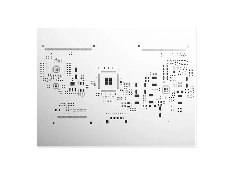
The fabrication of PCB stencils relies on precise techniques to ensure accurate solder paste deposition. Two primary methods dominate: laser cutting and chemical etching. Each offers distinct advantages concerning precision, cost, and suitability for different production volumes. Understanding these methods is critical for selecting the appropriate stencil fabrication approach.
| Feature | Laser Cutting | Chemical Etching |
|---|---|---|
| Precision | High (±20μm or better) | Moderate (±50μm) |
| Cost | Moderate to High | Low to Moderate |
| Complexity | Can handle complex designs with fine features | Suitable for less intricate designs |
| Speed | Slower, especially for high density | Faster for simple designs |
| Material Compatibility | Works well with stainless steel and polyimide | Primarily used with stainless steel |
| Turnaround Time | Typically quick, but depends on design complexity | Usually quick, especially for volume |
| Edge Quality | Clean, sharp edges | Can have slightly rounded edges |
Laser cutting employs a focused laser beam to vaporize material, creating the desired aperture pattern on the stencil. This process excels in producing stencils with high precision, making it suitable for complex designs and fine-pitch components. The accuracy of laser-cut stencils significantly reduces the risk of soldering defects. The cost of laser cutting is typically higher than chemical etching, making it more suitable for high-precision applications, and when design complexity is high.
Chemical etching involves applying a photoresist to the stencil material, exposing it to UV light to create a pattern, and then using chemical etchants to remove the unprotected material. This method is cost-effective for producing less intricate stencils. Chemical etching is suitable for simpler designs, and for when cost effectiveness is the priority. However, the precision of the chemical etching is less accurate than that achieved by the laser cutting method, thus, it may not be the best choice for intricate designs.
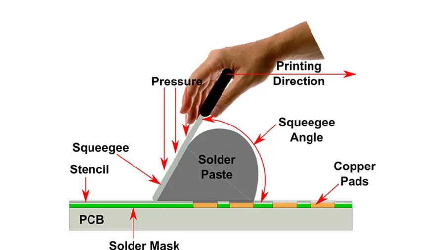
Accurate design of PCB stencils is paramount to ensure effective solder paste deposition, which directly impacts the reliability and quality of the final assembled printed circuit board. This involves careful consideration of aperture size and alignment features, each playing a vital role in minimizing soldering defects. This section delves into the critical aspects of aperture design and alignment methods.
The primary design considerations for PCB stencils are focused on ensuring a precise transfer of solder paste onto the printed circuit board pads. This is achieved by meticulous design of the apertures and alignment features, minimizing the chances of solder bridging, insufficient solder, and misaligned components.
Careful attention to aperture design and accurate alignment are vital for achieving high-quality solder joints, this meticulous approach will decrease the rework rates on PCBs and enhance overall manufacturing yield, and reduce overall costs. By focusing on these essential design elements, engineers can reduce manufacturing defects, enhance the overall quality, and improve long term reliability of the electronic devices produced.
Selecting the appropriate PCB stencil maker is crucial for ensuring the accuracy and reliability of your surface mount technology (SMT) assembly process. This decision directly impacts the quality of solder paste deposition, which is a cornerstone of successful electronic device manufacturing. A careful evaluation of several key factors is essential to achieve optimal outcomes.
This section addresses common questions about PCB stencils and the role of PCB stencil makers, providing practical insights and comprehensive explanations to assist users in understanding the nuances of stencil fabrication and application.
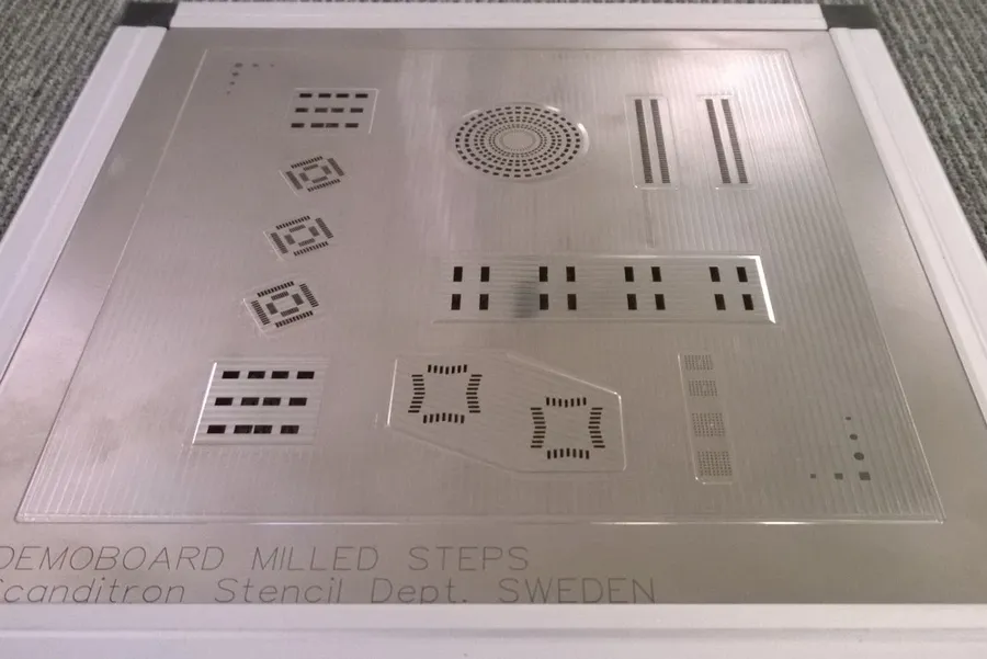
Advanced PCB stencil techniques, such as step-up and step-down stencils, are crucial for optimizing solder paste deposition in complex Surface Mount Technology (SMT) assemblies. These specialized stencils address challenges arising from varying component heights and pad sizes on a single circuit board, ensuring consistent and reliable solder joints.
| Stencil Type | Description | Use Case | Advantages | Disadvantages |
|---|---|---|---|---|
| Step-Up Stencil | Stencil thickness is increased in specific areas. | Accommodating larger components with larger solder volumes. | Ensures adequate solder paste for larger components; reduces tombstoning and insufficient solder issues. | Can be more complex to manufacture; may require multiple passes for precise paste deposition. |
| Step-Down Stencil | Stencil thickness is reduced in specific areas. | Accommodating smaller components with smaller solder volumes. | Prevents excess solder paste on smaller pads; reduces bridging and solder balling. | Can result in inconsistent solder volume if not manufactured accurately; may require special squeegee settings. |
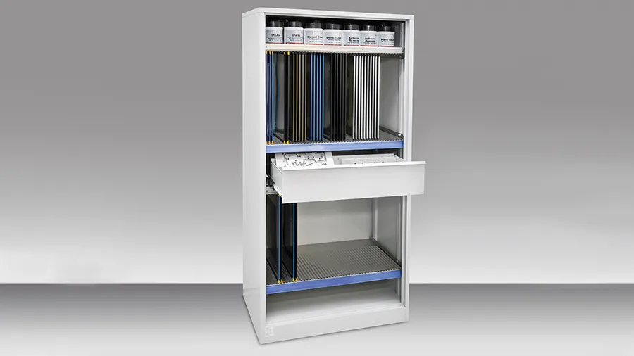
Proper maintenance and storage of PCB stencils are crucial for ensuring their continued performance and extending their lifespan, ultimately safeguarding the precision of your surface mount assembly process. Neglecting these steps can lead to diminished print quality and increased defects.
The role of a PCB stencil maker is pivotal in the modern electronics manufacturing process. Selecting the right stencil, understanding material and fabrication options, and considering the design details are all key to achieving reliable, high-quality SMT assemblies. By understanding these factors, you'll be well-equipped to navigate the choices offered by PCB stencil makers, ensuring your projects benefit from precise and consistent solder paste application. From prototype stages to large scale production, the careful consideration of PCB stencils, and the selection of the right PCB stencil maker, directly impacts the quality of finished devices.

