In an increasingly interconnected world, precise positioning and navigation are paramount. From autonomous vehicles to precision agriculture and critical infrastructure, satellite navigation receivers form the backbone of countless innovations. The performance of these receivers, however, hinges critically on the underlying Printed Circuit Board (PCB) solution. At Zero One Solution Limited, we understand that a superior PCB is not just a component, but the very foundation for exceptional signal integrity, power efficiency, and robust operation. As a leading PCB solution provider with a decade of experience, we're here to delve into how our comprehensive Satellite Navigation Receiver PCB Solutions empower next-generation GNSS applications, accelerating your journey from concept to market.
The Critical Role of PCBs in Satellite Navigation Receivers
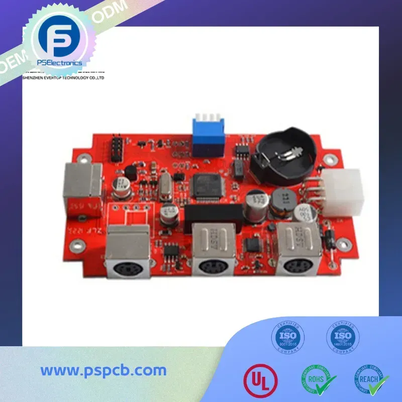
Satellite Navigation Receiver PCB
The Printed Circuit Board (PCB) serves as the fundamental backbone of any high-performance satellite navigation receiver, a cornerstone component whose integrity profoundly influences signal acquisition, processing accuracy, and overall system reliability in Global Navigation Satellite System (GNSS) applications. Its meticulous design and fabrication are paramount to mitigating signal loss, managing complex power distribution, and ensuring the robust operation of sensitive RF components. Zero One Solution Limited specializes in overcoming the unique engineering challenges inherent in these critical PCBs, delivering solutions that uphold the highest standards of precision and resilience required for advanced navigation.
Signal Integrity and Precision The intricate routing of RF traces on a satellite navigation receiver PCB directly impacts signal integrity. Any impedance mismatch, excessive trace length, or crosstalk can degrade the weak GNSS signals, leading to reduced accuracy or even complete signal loss. High-frequency design principles and precise impedance control are critical to maintaining the fidelity of these micro-volt signals, ensuring the receiver can accurately lock onto satellite transmissions and compute precise positioning data.
Power Management Efficiency Efficient power management is crucial for the longevity and performance of GNSS receivers, especially in portable or low-power applications. The PCB must accommodate diverse power domains, from sensitive analog RF front-ends to high-speed digital processors, ensuring stable voltage supplies and minimizing power consumption. Effective power plane design and decoupling strategies prevent noise propagation that could corrupt sensitive signals, extending battery life and enhancing operational reliability.
Thermal Dissipation and Component Stability Modern GNSS chipsets and associated components generate heat, which can negatively impact performance and long-term reliability if not adequately managed. The PCB acts as a primary heat sink, and its material selection and layout must facilitate efficient thermal dissipation. Proper thermal management prevents performance degradation due to temperature fluctuations, ensuring consistent operation across varying environmental conditions and extending the lifespan of critical components. For instance, a 10°C increase in operating temperature can halve the lifespan of certain integrated circuits.
Miniaturization and Form Factor With the increasing demand for compact and lightweight GNSS devices, the PCB design must support high-density integration. This requires advanced manufacturing techniques such as HDI (High-Density Interconnect) and precise component placement. Achieving a small form factor without compromising performance presents significant challenges in maintaining signal isolation, managing thermal loads, and ensuring manufacturability. Zero One Solution Limited leverages its expertise in these areas to deliver compact yet robust PCB solutions for diverse applications.
Environmental Resilience Satellite navigation receivers often operate in harsh environments, from extreme temperatures to high humidity and vibration. The PCB materials and surface finishes must be selected to withstand these conditions, ensuring long-term durability and consistent performance. This includes choosing substrates with low moisture absorption and utilizing robust conformal coatings to protect against environmental contaminants, ensuring the receiver maintains operational integrity in challenging scenarios.
Key Design Considerations for High-Precision GNSS Receiver PCBs
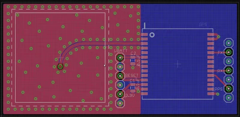
GNSS Receiver PCB Design
Designing Printed Circuit Boards (PCBs) for high-precision Global Navigation Satellite System (GNSS) receivers is a highly specialized discipline that directly impacts the accuracy, reliability, and overall performance of the navigation system. These PCBs are not merely platforms for components; they are integral to managing sensitive RF signals, mitigating interference, and ensuring stable operation under diverse conditions. Mastering critical design considerations such as RF signal integrity, precise impedance control, effective noise reduction, and robust thermal management is paramount for achieving the sub-meter or even centimeter-level accuracy demanded by modern GNSS applications. Zero One Solution Limited's extensive experience in rapid prototyping and advanced manufacturing ensures these intricate requirements are met, transforming complex designs into high-performance realities.
RF Signal Routing and Integrity The core challenge in GNSS PCB design is the meticulous handling of weak, high-frequency satellite signals. This necessitates short, direct, and symmetrical RF traces to minimize signal loss and phase distortion. Proper microstrip or stripline configurations with controlled characteristic impedance (typically 50 ohms) are crucial to prevent reflections and ensure maximum power transfer. Isolation between RF sections and digital circuitry is also vital to prevent interference that could degrade signal-to-noise ratio (SNR).
Impedance Control Maintaining precise impedance across all high-frequency traces is non-negotiable for signal integrity. Any deviation can lead to signal reflections, standing waves, and ultimately, a reduced effective signal strength for the GNSS receiver. This requires careful material selection (dielectric constant, loss tangent), precise trace width and spacing, and accurate stack-up design, often necessitating specialized PCB manufacturing processes to achieve tight tolerances (e.g., ±5%).
Noise Reduction and Shielding GNSS receivers are highly susceptible to noise from internal digital circuits, power supplies, and external electromagnetic interference (EMI). Effective noise reduction strategies include robust grounding schemes (e.g., solid ground planes), strategic placement of decoupling capacitors, proper power supply filtering, and the use of shielding techniques (e.g., guard rings, Faraday cages, or shielded enclosures) to isolate sensitive analog RF paths from noisy digital sections. Careful component placement also minimizes cross-talk and inductive coupling.
Zero One Solution Limited's Comprehensive PCB Solution for Satellite Navigation
Satellite Navigation PCB Assembly
Zero One Solution Limited offers a comprehensive, integrated PCB solution meticulously engineered to meet the exacting demands of satellite navigation receivers. Our end-to-end service encompasses every phase from initial design and layout optimization to advanced manufacturing and final assembly, ensuring a seamless and accelerated development cycle for complex Global Navigation Satellite System (GNSS) devices. This holistic approach, powered by our rapid prototyping capabilities, significantly reduces time-to-market and fosters innovation in the critical satellite navigation domain.
Integrated Design & Layout We provide expert PCB design and layout services specifically tailored for satellite navigation receivers, focusing on optimizing RF signal integrity, minimizing noise, and ensuring precise component placement. Our engineers leverage decades of experience to navigate the complexities of high-frequency and sensitive circuitry essential for accurate GNSS performance, translating your conceptual designs into robust, manufacturable layouts. This includes meticulous impedance control and power delivery network (PDN) optimization to maintain signal fidelity crucial for receiver accuracy and sensitivity.
Advanced Materials and Manufacturing Techniques for Optimal Performance
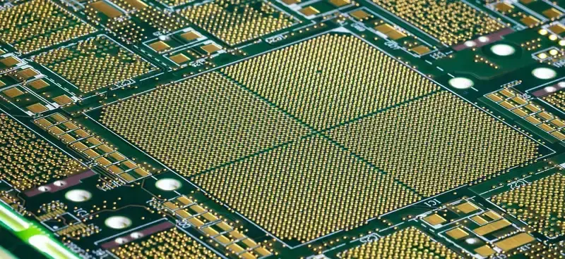
High-Density Interconnect PCB
Achieving optimal performance in Satellite Navigation Receiver PCBs necessitates the strategic selection of advanced materials and the application of cutting-edge manufacturing techniques. These critical choices directly impact signal integrity, power efficiency, and the miniaturization required for compact GNSS devices, ensuring superior precision and reliability in demanding environments.
Material Property
Benefit for GNSS PCB
Common Material Examples
Low Dielectric Loss (Df)
Minimizes signal attenuation at high frequencies, crucial for maintaining strong GNSS signals.
Rogers RO4000 series, Arlon 25N
Stable Dielectric Constant (Dk)
Ensures consistent impedance control and predictable signal propagation across varying frequencies and temperatures.
Teflon (PTFE), Liquid Crystal Polymer (LCP)
Low Coefficient of Thermal Expansion (CTE)
Reduces stress on components and vias during temperature cycling, enhancing long-term reliability.
BT-Epoxy, Polyimide
High Thermal Conductivity
Dissipates heat effectively from critical components, preventing performance degradation and extending lifespan.
Metal-Core PCBs (MCPCB), Ceramic-filled laminates
High-Density Interconnect (HDI) Technology HDI PCBs are fundamental for integrating the complex circuitry of modern GNSS receivers into smaller form factors. By utilizing microvias, buried vias, and fine lines/spaces, HDI technology enables higher component density and shorter signal paths, significantly reducing signal loss and improving overall electrical performance. This is crucial for miniaturized GNSS modules found in wearables, drones, and autonomous vehicles where space is at a premium and signal integrity cannot be compromised. Zero One Solution Limited leverages multi-layer HDI structures to optimize routing for sensitive RF and digital signals, minimizing crosstalk and electromagnetic interference (EMI).
Laser Drilling and Microvia Fabrication Precision laser drilling is essential for creating the minute microvias required in HDI structures. These tiny vias facilitate interconnectivity between layers in a highly compact manner, enabling advanced routing strategies for high-frequency signals. The ability to create extremely small and precise holes ensures optimal signal transmission and mechanical stability, which are paramount for the performance and durability of GNSS receiver PCBs. Our advanced laser drilling capabilities ensure superior accuracy and repeatability, critical for high-volume production of complex boards.
Quality Assurance and Testing for Robust Satellite Navigation Systems
PCB Quality Testing
In the demanding realm of satellite navigation, where precision and reliability are paramount, the underlying Printed Circuit Board (PCB) must exhibit flawless performance. Zero One Solution Limited implements rigorous quality assurance and comprehensive testing protocols to guarantee that every Satellite Navigation Receiver PCB manufactured is robust, durable, and consistently performs under diverse operational conditions, which is crucial for mission-critical GNSS applications. Our commitment to stringent quality control ensures the integrity of high-frequency signals and the longevity of your navigation systems.
What are the primary quality assurance measures for Satellite Navigation Receiver PCBs? Zero One Solution Limited employs a multi-faceted quality assurance framework. This begins with Design for Manufacturability (DFM) and Design for Testability (DFT) reviews to identify and mitigate potential issues early in the design phase. We then implement stringent Incoming Quality Control (IQC) for raw materials, In-Process Quality Control (IPQC) during manufacturing, and comprehensive Final Quality Control (FQC) before shipment. Key measures include visual inspection, automated optical inspection (AOI), X-ray inspection (AXI) for hidden solder joints, and electrical testing to verify circuit functionality and impedance control.
How does Zero One Solution Limited ensure signal integrity in Satellite Navigation Receiver PCBs through testing? Signal integrity is critical for GNSS receiver PCBs. We utilize advanced testing methodologies such as Time Domain Reflectometry (TDR) for precise impedance measurement and verification of transmission line characteristics. Network analyzers are employed to assess RF performance, including insertion loss, return loss, and isolation, ensuring optimal signal propagation and minimal distortion across the board. This meticulous approach guarantees that the PCB's electrical properties support high-precision satellite signal reception.
What environmental stress testing is performed on Satellite Navigation Receiver PCBs? To ensure durability and consistent performance in varied environments, Zero One Solution Limited conducts a range of environmental stress screenings. These include thermal cycling to simulate temperature fluctuations, humidity testing to assess resistance to moisture, and vibration testing to evaluate mechanical integrity under dynamic conditions. For specific critical applications, salt spray testing may also be performed to assess corrosion resistance. These tests are vital for PCBs operating in harsh outdoor or aerospace environments.
Are there specific certifications or standards Zero One Solution Limited adheres to for GNSS PCB manufacturing? Yes, Zero One Solution Limited adheres to internationally recognized quality management systems and industry standards relevant to high-reliability electronics manufacturing. This includes ISO 9001 for quality management, and compliance with IPC standards (e.g., IPC-A-600 for acceptability of PCBs and IPC-6012 for qualification and performance of rigid PCBs) which are crucial for ensuring the reliability and performance of Satellite Navigation Receiver PCBs. Our processes are designed to meet or exceed these stringent requirements.
How does Zero One Solution Limited address potential electromagnetic interference (EMI) in GNSS receiver PCB testing? EMI can significantly degrade the performance of sensitive GNSS receivers. Our testing protocols include comprehensive EMI/EMC (Electromagnetic Compatibility) pre-compliance testing to identify and mitigate potential interference sources. This involves evaluating the PCB's susceptibility to external noise and its own emissions. Through careful layout analysis and specialized testing equipment, we ensure that the PCB design effectively minimizes EMI, preserving the clarity and strength of satellite signals.
Case Studies: Success Stories in GNSS PCB Development
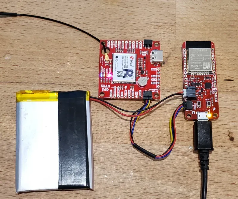
GNSS Device Prototype
Zero One Solution Limited's expertise in satellite navigation receiver PCB solutions is best demonstrated through real-world applications where our bespoke designs and rapid prototyping capabilities have enabled clients to achieve remarkable advancements in their GNSS technologies. Our collaborative approach and commitment to precision engineering consistently deliver superior performance and accelerate time-to-market for innovative navigation systems. These case studies underscore our proficiency in tackling complex challenges, from demanding signal integrity requirements to compact form factor integration, ultimately leading to successful product launches and enhanced operational capabilities for our partners.
Client Type
Challenge
Zero One Solution's Approach
Solution Provided
Impact/Outcome
Aerospace Manufacturer
Miniaturized, high-frequency GNSS receiver PCB for UAVs with strict weight and space constraints, requiring exceptional signal integrity in noisy environments.
Utilized HDI technology with low-loss dielectric materials (e.g., Rogers 4350B) and optimized stack-up for RF isolation. Implemented precision impedance control and advanced shielding techniques.
Delivered a multi-layer rigid-flex PCB with integrated antenna pathways and robust EMI suppression, maintaining signal fidelity at L1/L5 bands.
Reduced board size by 30% while improving navigation accuracy by 15%, enabling longer flight times and more reliable drone operations. Client secured major defense contract due to superior GNSS performance.
Client Type
Challenge
Zero One Solution's Approach
Solution Provided
Impact/Outcome
Automotive OEM
Developing a next-generation autonomous driving system requiring highly reliable, robust GNSS positioning in varied environmental conditions (temperature, vibration).
Produced a durable, multi-layer PCB designed for automotive environments, ensuring stable performance across wide temperature ranges and against mechanical stresses.
Achieved ASIL-B compliance for the GNSS module. Significantly reduced field failures by 20% and accelerated vehicle testing timelines, positioning the OEM as a leader in autonomous vehicle technology.
Client Type
Challenge
Zero One Solution's Approach
Solution Provided
Impact/Outcome
Marine Navigation System Developer
Need for a ruggedized, highly accurate GNSS receiver PCB capable of operating continuously in corrosive marine environments with minimal power consumption.
Selected specialized conformal coatings and corrosion-resistant finishes. Optimized power delivery networks (PDN) and implemented power-saving design techniques. Performed rigorous salt spray and humidity testing.
Engineered a robust, low-power PCB with enhanced environmental protection, ensuring long-term reliability and precision in maritime conditions.
Extended operational battery life by 25% and reduced maintenance costs by 10%. The system now provides uninterrupted, centimeter-level positioning even in challenging offshore scenarios, enhancing vessel safety and efficiency.
These success stories exemplify Zero One Solution Limited's commitment to delivering unparalleled PCB solutions for the demanding satellite navigation sector. By combining deep technical expertise with a client-centric approach, we empower our partners to innovate and succeed in a rapidly evolving global market.
Why Choose Zero One Solution Limited for Your Satellite Navigation Receiver PCB Needs?
For engineers and product developers seeking unparalleled reliability and efficiency in satellite navigation receiver PCB solutions, Zero One Solution Limited stands as the premier partner. Our comprehensive expertise, rapid prototyping capabilities, and global operational framework are specifically tailored to accelerate your product development cycles and ensure the highest performance for your GNSS applications. We bridge the gap between innovative design and flawless execution, offering a one-stop solution that minimizes complexities and maximizes your time to market.
Rapid Prototyping and Accelerated Development Our core strength lies in rapid-response R&D prototype manufacturing. We understand the critical need for speed in the competitive satellite navigation market. Our optimized processes and dedicated teams ensure that your design iterations are quickly transformed into functional prototypes, allowing for faster testing, validation, and ultimately, a significantly reduced development timeline for your satellite navigation receiver PCBs. This agility is crucial for staying ahead in a fast-evolving industry, enabling quicker product launches and market entry.
Integrated One-Stop PCB Solution Zero One Solution Limited provides a seamless, end-to-end service for satellite navigation receiver PCBs, covering every stage from initial design and layout to advanced manufacturing and final assembly. This integrated approach eliminates the complexities of coordinating multiple vendors, ensuring consistent quality, improved communication, and a streamlined supply chain. Our holistic service model means you can focus on innovation while we handle the intricate details of your PCB production, guaranteeing a cohesive and efficient project flow for your critical GNSS components.
Global Reach and Strategic Locations With our headquarters strategically located in Shenzhen, China – the heart of global electronic manufacturing – and a robust branch office in Dubai, we offer unparalleled access to a vast global PCBA supply chain network. These strategic locations provide significant advantages in sourcing high-quality materials, leveraging advanced manufacturing capabilities, and ensuring efficient logistics. This global footprint guarantees seamless access to worldwide resources and support, enabling us to deliver cost-effective and timely solutions for clients across continents, regardless of the complexity of their satellite navigation receiver PCB requirements.
Frequently Asked Questions About Satellite Navigation Receiver PCBs
Understanding the intricacies of Satellite Navigation Receiver PCBs is crucial for successful product development. This section addresses common inquiries, offering clear, concise answers to help you navigate the complexities of design, manufacturing, and performance of these critical components within GNSS applications.
What are the primary challenges in designing PCBs for high-precision satellite navigation receivers? Designing PCBs for high-precision satellite navigation receivers presents unique challenges primarily due to the need for extreme signal integrity and noise immunity. Key challenges include meticulous RF trace routing to minimize signal loss and interference, precise impedance control (typically 50 Ohms) to match antenna and RF front-end requirements, effective electromagnetic compatibility (EMC) to prevent interference from other components, and robust power delivery network (PDN) design to ensure stable voltage for sensitive RF and digital circuits. Thermal management is also critical for consistent performance, especially in compact or high-power designs.
Why are specialized materials important for Satellite Navigation Receiver PCBs? Specialized PCB materials are paramount for Satellite Navigation Receiver PCBs because they operate at high frequencies (L-band for GNSS signals). Standard FR-4 materials can exhibit higher dielectric loss at these frequencies, leading to signal attenuation and reduced receiver sensitivity. Low-loss dielectric materials, such as Rogers, Arlon, or other ceramic-filled laminates, offer lower dissipation factors, stable dielectric constants across varying temperatures, and improved impedance control. These properties are essential for preserving signal integrity, minimizing phase noise, and ultimately enhancing the accuracy and reliability of the GNSS receiver.
How does Zero One Solution Limited ensure signal integrity in GNSS receiver PCB designs? Zero One Solution Limited ensures superior signal integrity in GNSS receiver PCB designs through a multi-faceted approach. This includes precise impedance matching using advanced trace geometry and stack-up configurations, rigorous control of trace lengths and differential pairs to minimize skew, strategic placement of sensitive RF components to reduce coupling, and comprehensive grounding schemes to mitigate noise. We employ advanced simulation tools for pre-layout analysis (e.g., SI/PI analysis) and utilize high-frequency layout guidelines, such as proper via transitions and component isolation, to maintain optimal signal performance even in complex, multi-layer designs.
What kind of testing is performed on Satellite Navigation Receiver PCBs? Zero One Solution Limited conducts rigorous testing on Satellite Navigation Receiver PCBs to guarantee their robust performance. This includes Electrical Test (E-Test) for open/short circuits, Automated Optical Inspection (AOI) for visual defects, and X-ray inspection for internal layer alignment and solder joint quality. For RF performance, we perform network analyzer measurements (S-parameters) to verify impedance matching and insertion loss. Environmental Stress Screening (ESS), such as thermal cycling and vibration testing, is also applied to ensure durability under harsh operating conditions, crucial for mission-critical GNSS applications.
Can Zero One Solution Limited assist with rapid prototyping for new GNSS receiver designs? Absolutely. Zero One Solution Limited specializes in rapid prototyping for new GNSS receiver designs. Our integrated one-stop service, from design and layout to manufacturing and assembly, is specifically geared towards accelerating product development cycles. With advanced facilities in Shenzhen and a global supply chain, we can quickly turn around complex PCB prototypes, allowing engineers to validate their designs, iterate rapidly, and bring innovative GNSS solutions to market with exceptional efficiency. Our expertise ensures that even the most cutting-edge designs can be prototyped quickly and accurately.
The demands on satellite navigation receiver technology continue to escalate, driving the need for increasingly sophisticated and reliable PCB solutions. At Zero One Solution Limited, we don't just provide PCBs; we deliver the foundation for your innovation in GNSS technology. Our commitment to rapid prototyping, design expertise, and a global supply chain ensures that your satellite navigation receiver products achieve optimal performance, reliability, and time-to-market. Partner with us to navigate the complexities of high-precision RF design and unlock the full potential of your next-generation satellite navigation applications. Visit our website or contact us today to discuss how our specialized Satellite Navigation Receiver PCB Solution can elevate your project.