In today's technology-driven world, the reliability of our electronic devices hinges on the quality of their components, and the charger PCB, acting as the vital energy bridge, is no exception. From mobile phones to electric vehicles, effective charging solutions are indispensable. Understanding the crucial role a charger PCB manufacturer plays in this ecosystem is paramount. This article delves into the key factors in choosing the right partner and navigating the critical design and manufacturing process of charger PCBs.
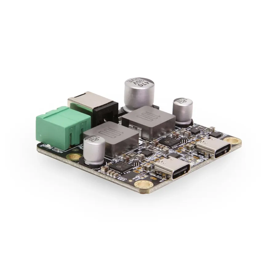
A charger Printed Circuit Board (PCB) is the foundational element of any electronic charging device, responsible for safely and efficiently converting electrical power from a source to a battery or other load. It encompasses a layered structure, with each layer serving a distinct purpose, utilizing specific materials like FR4 and CEM1, and relying on copper traces for conductive pathways, all of which critically impact the charger's performance.
The performance of a charger PCB is directly influenced by its core components and design. These include:
Selecting the right charger PCB manufacturer is crucial for ensuring product quality, reliability, and performance. This decision hinges on several critical factors beyond just cost, encompassing the manufacturer's capabilities, certifications, quality control, and experience. A comprehensive evaluation of these aspects is essential for a successful partnership.
| Factor | Importance |
|---|---|
| Manufacturing Capabilities | Ensures technical requirements are met. |
| Certifications (ISO) | Indicates adherence to quality and environmental standards. |
| Quality Control Processes | Guarantees consistent and reliable PCB performance. |
| Industry Experience | Demonstrates specialized knowledge in relevant applications. |
| Prototype and Mass Production Support | Facilitates design verification and scalable production. |
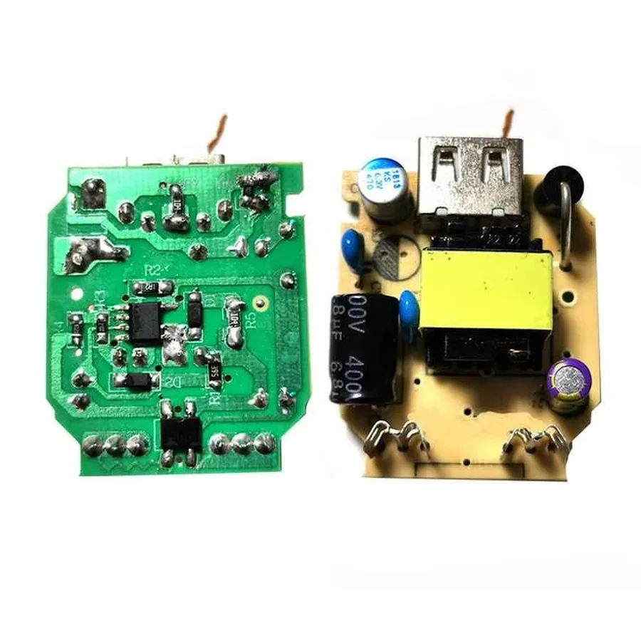
A critical aspect of selecting a charger PCB manufacturer is their ability to provide customized solutions that meet specific design requirements. This includes variations in size, shape, and the integration of advanced functionalities such as fast charging and wireless charging capabilities. A manufacturer's design support and engineering expertise are paramount in realizing these tailored designs.
| Customization Aspect | Description | Considerations |
|---|---|---|
| Size and Shape | Tailoring the PCB dimensions and form factor to fit specific device enclosures. | Ensures seamless integration within the final product. |
| Functionality | Incorporating specialized circuits for fast charging, wireless charging, or other unique features. | Requires expertise in advanced circuit design and signal integrity. |
| Layer Count | Adjusting the number of PCB layers to accommodate complex routing and component placement. | Directly impacts PCB complexity, cost, and performance. |
| Material Selection | Choosing materials with specific thermal and electrical properties to meet performance requirements. | Affects the PCB's durability, heat dissipation, and signal transmission. |
| Component Layout | Optimizing the physical arrangement of components on the PCB to minimize signal interference and improve overall efficiency. | Demands a clear understanding of circuit behavior and space constraints. |
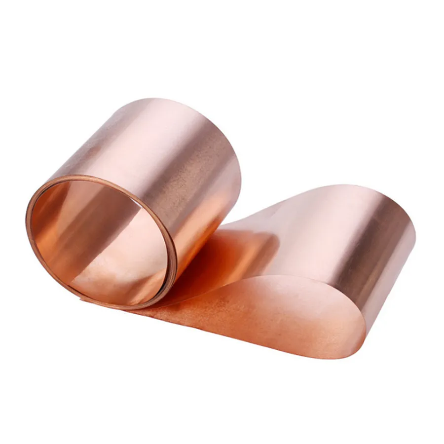
The selection of materials is paramount in determining the performance, durability, and reliability of a charger PCB. This section will delve into the common materials, such as FR4 and CEM1, used in charger PCB manufacturing, analyzing their properties and suitability for various applications. Understanding these materials is crucial for selecting a manufacturer that can meet specific performance requirements.
| Material | Composition | Pros | Cons | Typical Applications |
|---|---|---|---|---|
| FR4 | Glass fiber reinforced epoxy laminate | Good balance of strength, cost, and electrical properties. Widely available and easy to manufacture. | Moderate thermal resistance, can be less suitable for high-temperature applications. | General-purpose chargers, mobile phone chargers, consumer electronics. |
| CEM1 | Paper reinforced epoxy laminate | More cost-effective than FR4. Good for applications with less stringent performance needs. | Lower mechanical strength and moisture resistance compared to FR4. Not ideal for harsh environments. | Low-cost chargers, less demanding applications. |
| High Tg FR4 | FR4 with higher glass transition temperature | Improved thermal performance, maintains mechanical integrity at higher temperatures. | More expensive than standard FR4. | Fast chargers, high-power chargers. |
| Aluminum Substrates | Aluminum base with dielectric layer. | Excellent heat dissipation, higher power handling, rigid construction. | More expensive than FR4 or CEM1, can be heavier. | EV chargers, high-power industrial chargers |
Beyond the base substrate materials, copper is fundamental for conducting electricity and creating circuits on the PCB. The thickness of the copper layer, measured in ounces per square foot, directly impacts current carrying capacity and heat dissipation. Thicker copper layers are preferred for high-current applications, such as fast charging, to minimize resistive losses and prevent overheating.
Additionally, the choice of solder mask and surface finish is critical. Solder mask protects the copper traces from oxidation and shorts, while the surface finish improves solderability and protects the copper from corrosion. Common surface finishes include HASL (Hot Air Solder Leveling), ENIG (Electroless Nickel Immersion Gold), and OSP (Organic Solderability Preservative), each offering varying levels of protection, solderability, and cost.
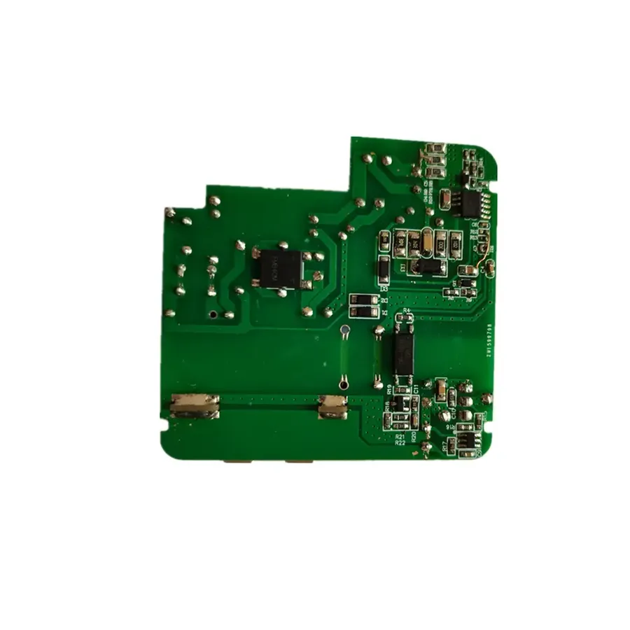
The design of a Printed Circuit Board (PCB) for fast charging differs significantly from that of a slow charging PCB, primarily due to the higher power demands and thermal management requirements of fast charging. These differences impact component selection, material properties, and overall layout, influencing the manufacturer’s process.
| Feature | Slow Charging PCB | Fast Charging PCB |
|---|---|---|
| Copper Trace Width | Narrower traces for lower current | Wider traces for higher current handling |
| Copper Thickness | Standard copper thickness (e.g., 1oz) | Thicker copper (e.g., 2oz or higher) for reduced resistance and heat generation |
| Thermal Vias | Few or no thermal vias | Extensive thermal vias to dissipate heat from high power components. |
| Component Selection | Standard components | Lower ESR capacitors, low RDS(on) MOSFETs to minimize power loss and heat |
| Layer Count | Often fewer layers. | May require additional layers to optimize signal integrity and thermal management. |
| Material Selection | Standard FR-4 | Advanced materials with higher thermal conductivity, like metal core PCB or modified FR4. |
These design choices directly influence heat dissipation, power handling capacity and overall efficiency. For fast charging PCBs, the manufacturer must ensure precise trace width and spacing, accurate component placement, and efficient thermal management techniques to handle high current and prevent potential issues.
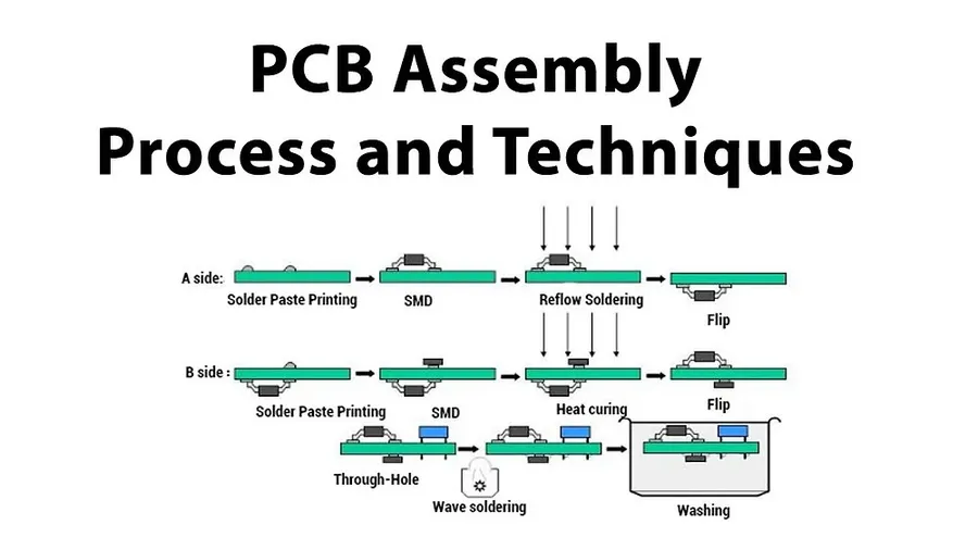
Printed Circuit Board Assembly (PCBA) services represent a critical step in the manufacturing process of charger PCBs, transforming bare boards into fully functional electronic components. PCBA encompasses the procurement of all necessary electronic components, such as integrated circuits (ICs), resistors, capacitors, and inductors, followed by their precise placement and soldering onto the fabricated PCB. The integration of PCBA services with PCB fabrication streamlines production, ensuring a cohesive and efficient manufacturing operation.
Selecting a manufacturer that offers both PCB fabrication and PCBA provides significant advantages, including reduced lead times, simplified supply chain management, and enhanced quality control. This integrated approach allows for seamless transition between the fabrication and assembly stages, minimizing potential errors and ensuring consistent product quality.
| Advantage | Description |
|---|---|
| Simplified Supply Chain | Reduces the number of vendors involved, streamlining logistics and communication. |
| Reduced Lead Times | Eliminates delays caused by coordinating between separate PCB fabrication and assembly providers. |
| Enhanced Quality Control | Enables a unified quality control process, ensuring consistent quality throughout both PCB fabrication and assembly. |
| Cost Efficiency | Often results in cost savings due to bundled services and reduced logistical overhead. |
| Improved Compatibility | Ensures that the assembly process is optimized for the specific PCB design, leading to higher yields and fewer assembly-related issues. |
The cost of producing charger PCBs is influenced by a variety of interconnected factors, encompassing material selection, manufacturing complexity, order volume, and lead time. Effectively balancing these elements is critical to achieving cost-effective, high-quality PCB production.
| Cost Factor | Description | Impact on Cost |
|---|---|---|
| Material Costs | The price of raw materials like FR4, CEM1, copper, and solder mask directly affects the overall cost. | Higher cost materials increase the final PCB price. |
| Manufacturing Complexity | Factors like the number of layers, via type (blind, buried), trace width, and minimum spacing between traces all contribute to complexity. | Increased complexity leads to higher production costs due to more intricate manufacturing processes. |
| Order Volume | The quantity of PCBs ordered has a significant effect on the per-unit cost. | Larger order volumes generally reduce the per-unit cost due to economies of scale. |
| Turnaround Time | The time required for PCB production can impact cost, especially expedited or rush orders. | Faster turnaround times usually incur higher fees due to accelerated production and resource allocation. |
| Surface Finish | Different surface finishes such as ENIG (Electroless Nickel Immersion Gold) or HASL (Hot Air Solder Leveling) have varying costs. | Higher cost finishes provide better performance and durability. |
| Testing Requirements | The level of testing required (e.g., AOI, flying probe, functional testing) can affect costs | More rigorous testing increases cost but provides greater assurance of quality and functionality |
| Design Requirements | Specific design requirements, such as impedance control, high-speed routing, and special plating, add to the manufacturing complexity. | More complex designs typically lead to increased costs. |
This section addresses common questions regarding charger PCBs, providing clear answers to guide your understanding and decision-making when selecting a manufacturer.
The landscape of charger PCB technology is rapidly evolving, driven by demands for higher efficiency, faster charging, and greater integration of smart features. These advancements are significantly impacting the design and manufacturing processes of PCBs, pushing manufacturers to adopt innovative materials and techniques.
Choosing the right charger PCB manufacturer is a critical decision that can significantly affect the performance and reliability of your products. By considering factors such as manufacturing capabilities, customization options, material quality, and cost-effectiveness, you can ensure a strong partnership with a manufacturer that meets your needs. As technology continues to evolve, staying informed about the latest trends in charger PCB technology and understanding the nuances in the manufacturing process will become ever more critical to remain competitive and provide cutting-edge products. Remember, a robust and efficient charger PCB is the backbone of any power solution, thus requiring careful selection of the ideal charger pcb manufacturer.

