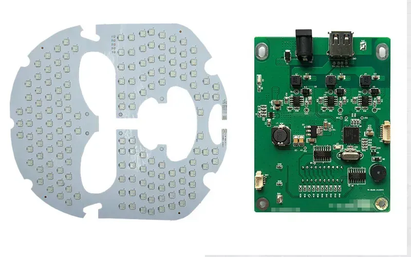
In today's beauty industry, shared beauty devices are revolutionizing how consumers experience skincare and cosmetic treatments. From high-frequency facial wands to LED therapy masks, these devices demand sophisticated PCB (Printed Circuit Board) solutions to ensure performance, safety, and reliability. Zero One Solution Limited stands at the forefront, providing cutting-edge PCB solutions tailored for the unique needs of shared beauty device manufacturers. But what makes a PCB solution truly effective for these devices, and how can manufacturers leverage these solutions to gain a competitive edge? Let's explore the critical aspects of PCB design, manufacturing, and assembly in the context of shared beauty devices.
The Rise of Shared Beauty Devices: A PCB Perspective
The shared beauty device market is experiencing remarkable growth, driven by increasing consumer demand for accessible and cost-effective beauty solutions. Printed circuit boards (PCBs) are at the heart of these devices, providing the essential electronic foundation for their functionality and safety. From portable facial cleansing brushes to sophisticated light therapy devices, the performance and reliability of shared beauty devices depend heavily on the quality and design of their PCBs.
Several factors contribute to the expansion of the shared beauty device sector:
Accessibility and Affordability: Shared devices lower the barrier to entry for advanced beauty treatments, making them available to a broader audience.
Technological Advancements: Continuous innovation in beauty technology allows for the development of more effective and user-friendly devices.
Changing Consumer Preferences: Consumers are increasingly seeking convenient and personalized beauty solutions that fit their lifestyles.
The Impact of PCB: The PCB is the core component of all electronic beauty equipment, its performance determines the stability, safety and function of the beauty equipment. Therefore, the performance of beauty equipment PCB requirements are higher.
The PCB’s role extends beyond basic electrical connectivity. It is crucial for:
Power Management: Efficiently distributing power to various components while minimizing heat generation.
Signal Integrity: Ensuring clear and reliable signal transmission for accurate and consistent performance.
Safety: Implementing safety features to prevent electrical hazards and ensure user protection.
Miniaturization: Enabling compact designs for portable and handheld devices.
As the shared beauty device market continues to evolve, the importance of high-quality, reliable PCBs will only increase. Zero One Solution Limited is committed to providing cutting-edge PCB solutions that meet the unique demands of this dynamic industry.
Key Requirements for PCBs in Shared Beauty Devices
PCBs in shared beauty devices must adhere to stringent requirements to ensure performance, safety, and user satisfaction. Miniaturization to fit sleek designs, effective thermal management to prevent overheating, and maintained signal integrity for reliable functionality are paramount. Biocompatibility is crucial to prevent adverse skin reactions, making material selection a critical consideration.
Miniaturization Shared beauty devices often require compact designs for portability and ease of use. PCBs must be highly miniaturized, utilizing advanced technologies such as HDI (High-Density Interconnect) to accommodate complex circuitry in a small area. This enables sleeker device designs and enhanced user experience.
Thermal Management Many beauty devices generate heat during operation. Effective thermal management is essential to prevent overheating, which can damage sensitive components and cause discomfort or injury to the user. PCBs should be designed with thermal vias, heat sinks, and appropriate materials to dissipate heat efficiently and maintain a stable operating temperature.
Signal Integrity Beauty devices often incorporate sensitive sensors and circuits that require high signal integrity for accurate and reliable performance. PCBs must be designed to minimize signal loss, noise, and interference. Controlled impedance, proper grounding, and shielding techniques are crucial to maintain signal integrity and ensure the device functions as intended.
Biocompatibility Shared beauty devices come into direct contact with the user's skin. PCBs must be made from biocompatible materials that do not cause allergic reactions, irritation, or other adverse effects. Materials should be compliant with relevant standards and regulations, such as ISO 10993, to ensure safety and prevent harm to the user.
Durability and Reliability Shared beauty devices are often subjected to frequent use and handling. PCBs must be durable and reliable to withstand the rigors of daily use. Robust design, high-quality materials, and rigorous testing are essential to ensure long-term performance and prevent premature failure. This includes resistance to moisture, cleaning agents, and physical stress.
Power Efficiency Many shared beauty devices are battery-powered. PCBs must be designed to minimize power consumption and maximize battery life. Low-power components, efficient power management circuits, and optimized routing techniques are crucial to extend the device's operating time and reduce the need for frequent charging or battery replacement.
Zero One Solution's Expertise in Beauty Device PCB Solutions
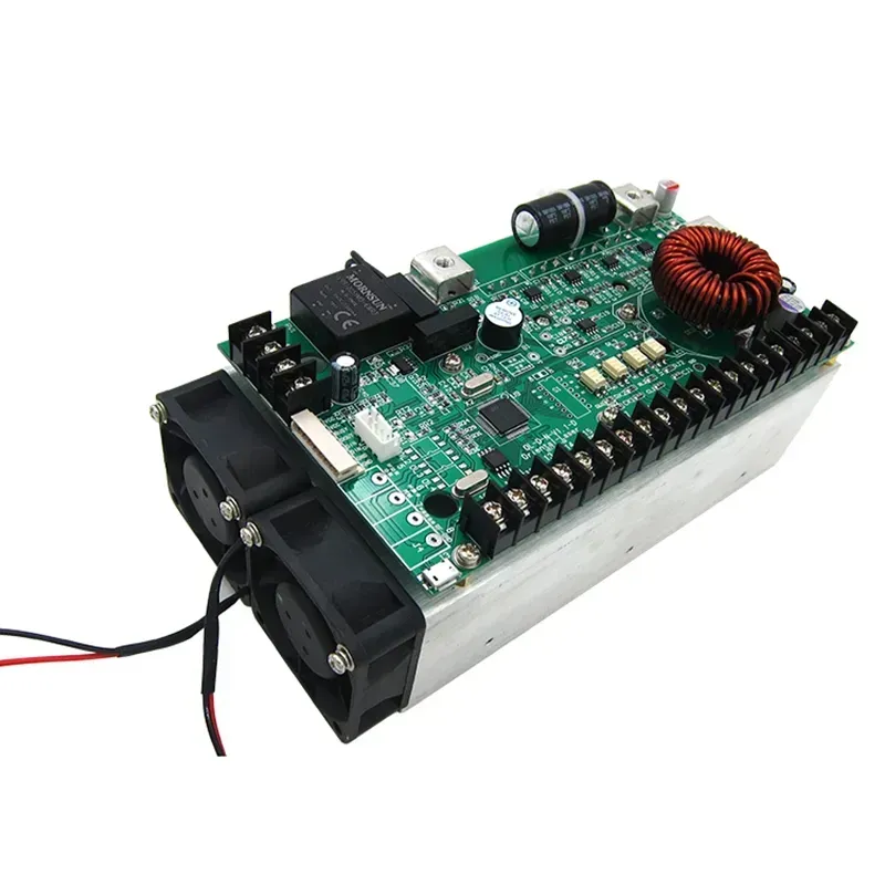
Beauty Device PCB Board
Zero One Solution Limited stands at the forefront of PCB solutions for shared beauty devices, leveraging years of expertise to deliver unparalleled services in design and manufacturing. Our profound understanding of the beauty device industry's unique demands allows us to provide tailored PCB solutions that optimize device performance, ensure safety, and accelerate time-to-market. We are committed to empowering our clients with cutting-edge PCB technology, enabling them to create innovative and effective beauty devices.
Comprehensive PCB Design Services Zero One Solution offers a complete suite of PCB design services, from initial concept to final layout, optimized for the specific requirements of shared beauty devices. We utilize advanced design tools and methodologies to ensure signal integrity, thermal management, and miniaturization, critical for high-performance beauty applications.
Advanced Manufacturing Capabilities Our state-of-the-art manufacturing facilities are equipped to handle complex PCB fabrication, including flexible PCBs, HDI (High-Density Interconnect) PCBs, and the integration of biocompatible materials. We maintain rigorous quality control standards throughout the manufacturing process to guarantee the reliability and longevity of our PCBs.
Rapid Prototyping Services Understanding the importance of speed in the beauty device market, we offer rapid prototyping services that allow clients to quickly iterate on their designs and accelerate product development. Our fast-turnaround times enable manufacturers to test and refine their devices, reducing time-to-market and gaining a competitive edge.
Material Selection Expertise We possess in-depth knowledge of PCB materials suitable for beauty applications, including biocompatible options that meet stringent safety standards. Our material selection expertise ensures that our PCBs are safe for skin contact and can withstand the demands of regular use.
Customized Solutions Zero One Solution provides customized PCB solutions tailored to the specific needs of each client's beauty device. Whether it's a handheld device or a larger stationary unit, we can design and manufacture PCBs that meet the unique performance and safety requirements of the application.
Quality Assurance and Testing We adhere to strict quality assurance protocols and conduct thorough testing at every stage of the PCB manufacturing process. Our testing procedures include electrical testing, impedance testing, and environmental testing to ensure that our PCBs meet the highest standards of quality and reliability.
Global Supply Chain Support With strategic locations in Shenzhen and Dubai, Zero One Solution offers efficient supply chain management and access to a global network of resources. We provide seamless support to beauty device manufacturers worldwide, ensuring timely delivery and cost-effective solutions.
Rapid Prototyping for Accelerated Beauty Device Development
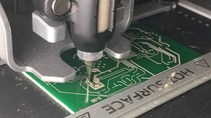
PCB Rapid Prototyping
In the fast-paced beauty device industry, rapid prototyping is crucial for quickly testing and refining designs. Zero One Solution Limited's fast-turnaround services enable beauty device manufacturers to iterate rapidly, significantly reducing time-to-market and gaining a competitive edge. Our expertise in PCB design, manufacturing, and assembly allows for the creation of functional prototypes that closely mimic the final product, ensuring accurate testing and validation.
What are the key benefits of rapid prototyping for beauty devices? Rapid prototyping helps in early detection of design flaws, accelerates the testing of new features, and allows for faster iteration cycles, ultimately reducing time-to-market and development costs. It also enables manufacturers to quickly adapt to changing market demands and incorporate user feedback.
How does Zero One Solution Limited facilitate rapid prototyping? Zero One Solution Limited offers fast-turnaround PCB fabrication and assembly services specifically tailored for rapid prototyping. Our streamlined processes, advanced equipment, and experienced engineers enable us to deliver high-quality prototypes in a fraction of the time compared to traditional methods.
What types of PCBs can be rapidly prototyped for beauty devices? We support rapid prototyping for a wide range of PCB types, including rigid PCBs, flexible PCBs, HDI PCBs, and multi-layer PCBs. This flexibility allows beauty device manufacturers to test various designs and functionalities without limitations.
What design considerations are important for rapid prototyping PCBs in beauty devices? Key considerations include component selection, thermal management, signal integrity, and manufacturability. Our engineers work closely with clients to optimize designs for rapid prototyping, ensuring that the prototypes accurately reflect the intended performance and functionality of the final product.
How does rapid prototyping contribute to cost savings in beauty device development? By identifying and addressing design flaws early in the development process, rapid prototyping helps prevent costly rework and redesigns later on. This iterative approach ensures that the final product meets the desired specifications and performance requirements, minimizing wasted resources and maximizing efficiency.
Can Zero One Solution Limited assist with component sourcing for rapid prototypes? Yes, we offer comprehensive component sourcing services to ensure that all necessary components are readily available for rapid prototyping. Our extensive network of suppliers and our expertise in component selection enable us to quickly procure high-quality components at competitive prices.
What level of testing and validation is performed on rapid prototypes? We offer a range of testing and validation services for rapid prototypes, including functional testing, performance testing, and environmental testing. These tests ensure that the prototypes meet the required specifications and perform reliably under various conditions, providing valuable insights for further design refinements.
Advanced PCB Materials and Technologies for Beauty Applications
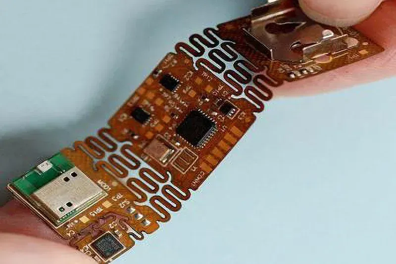
Flexible PCB Circuit Board
The efficacy and safety of shared beauty devices hinge significantly on the materials and technologies employed in their Printed Circuit Boards (PCBs). This section explores the diverse range of materials and cutting-edge technologies that Zero One Solution leverages to create high-performance PCBs tailored for the demanding requirements of beauty applications. These include flexible PCBs for intricate designs, HDI PCBs for miniaturization, and biocompatible coatings to ensure user safety and device longevity.
Here's a detailed look at some of the key materials and technologies:
Flexible PCBs Flexible PCBs utilize materials like polyimide films, enabling them to bend and conform to complex shapes within compact beauty devices. This is crucial for devices requiring intricate designs and high component density. They enhance durability, reduce weight, and improve overall device aesthetics.
High-Density Interconnect (HDI) PCBs HDI PCBs feature finer lines and spaces, microvias, and advanced materials, allowing for increased component density and improved signal integrity in smaller form factors. This technology is essential for sophisticated beauty devices that require complex circuitry in a limited space. They also support faster data transmission and reduced power consumption.
Biocompatible Coatings Ensuring user safety is paramount. Biocompatible coatings, such as Parylene or other specialized materials, are applied to PCBs to prevent allergic reactions or skin irritation during device use. These coatings provide a barrier against moisture, chemicals, and other environmental factors, enhancing the device's lifespan and safety profile.
Rogers Materials Rogers high-frequency laminates offer superior electrical performance, low signal loss, and excellent thermal management capabilities. These materials are ideal for beauty devices that utilize radio frequency (RF) technologies, such as skin tightening or hair removal devices, ensuring consistent and reliable performance.
Metal Core PCBs (MCPCB) MCPCBs incorporate a metal core, typically aluminum, to efficiently dissipate heat away from critical components. This is particularly important in beauty devices that generate heat during operation, such as laser or LED-based devices, preventing overheating and ensuring stable performance.
Zero One Solution Limited meticulously selects and integrates these advanced materials and technologies to deliver PCB solutions that meet the stringent performance, safety, and reliability requirements of shared beauty devices. Our expertise ensures that your devices not only function flawlessly but also adhere to the highest standards of user safety and product longevity.
Ensuring Quality and Reliability in Beauty Device PCBs
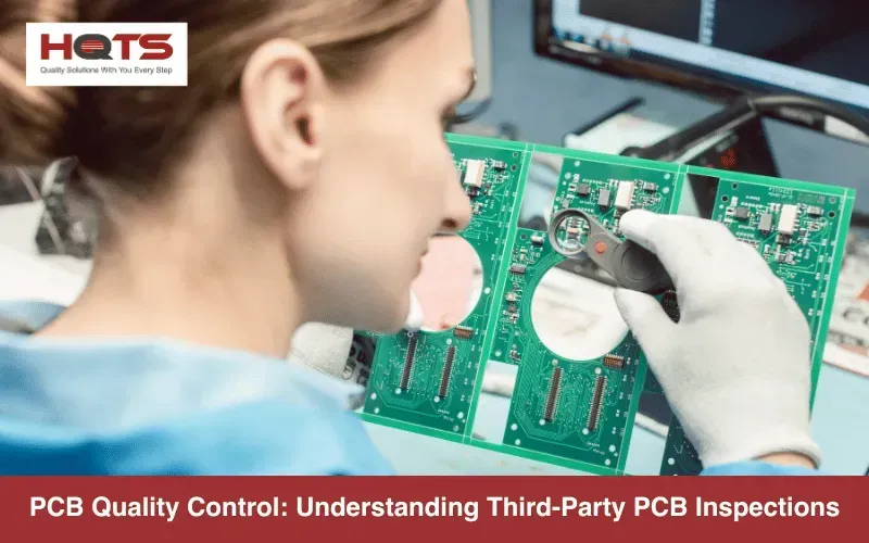
PCB Board Quality Inspection
Ensuring the quality and reliability of PCBs used in shared beauty devices is paramount, as these devices often come into direct contact with the skin and are used repeatedly by different individuals. Zero One Solution Limited implements stringent quality control measures and testing procedures throughout the PCB design, manufacturing, and assembly processes to guarantee the safety, performance, and longevity of our beauty device PCBs.
What quality control measures are implemented during the PCB manufacturing process for beauty devices? Zero One Solution Limited employs a multi-stage quality control process, including Automated Optical Inspection (AOI), X-ray inspection, and functional testing to identify and eliminate defects at each stage of production. We adhere to IPC standards and utilize advanced testing equipment to ensure that our PCBs meet the highest quality standards.
What types of testing procedures are used to ensure the reliability of beauty device PCBs? We conduct a range of reliability tests, including thermal cycling, vibration testing, and humidity testing, to simulate the real-world conditions that beauty devices may encounter. These tests help us identify potential failure points and ensure that our PCBs can withstand the rigors of regular use.
How does Zero One Solution Limited ensure the biocompatibility of PCBs used in beauty devices? We use biocompatible materials and surface finishes that are safe for skin contact. Our PCBs undergo rigorous testing to ensure they do not leach harmful substances or cause allergic reactions. We also work closely with our customers to select materials that meet their specific biocompatibility requirements.
What certifications does Zero One Solution Limited hold to demonstrate its commitment to quality? Zero One Solution Limited is ISO 9001 certified, demonstrating our commitment to quality management systems. We also comply with relevant industry standards, such as RoHS and REACH, to ensure that our products are environmentally friendly and safe for use.
How does Zero One Solution Limited handle customer complaints or issues related to PCB quality? We have a dedicated customer support team that handles all customer complaints and issues promptly and efficiently. We conduct thorough investigations to identify the root cause of the problem and implement corrective actions to prevent recurrence. We are committed to providing our customers with the highest level of satisfaction.
What traceability measures are in place to track the components and materials used in beauty device PCBs? We maintain full traceability of all components and materials used in our PCBs, allowing us to quickly identify and address any issues that may arise. Our traceability system includes detailed records of supplier information, batch numbers, and manufacturing dates.
How does Zero One Solution Limited stay up-to-date with the latest quality control standards and testing procedures? We invest in continuous training and development for our employees to ensure they are up-to-date with the latest quality control standards and testing procedures. We also actively participate in industry conferences and workshops to stay informed about emerging trends and best practices.
Supply Chain Optimization for Global Beauty Device Manufacturers
Zero One Solution Limited excels in optimizing the supply chain for global beauty device manufacturers through its strategic positioning in Shenzhen and Dubai. This dual-location advantage enables efficient supply chain management, reduces costs, and provides access to a comprehensive global network of resources, ensuring clients receive the best possible support from design to final product delivery.
Strategic Geographic Advantage Located in Shenzhen, the heart of China's electronics manufacturing hub, Zero One Solution benefits from proximity to a vast network of component suppliers, manufacturers, and logistics providers. Our Dubai branch further extends our reach, offering strategic access to markets in the Middle East, Africa, and Europe.
Cost-Effective Solutions By leveraging the efficiencies of our Shenzhen location, we provide cost-effective PCB manufacturing and assembly services without compromising on quality. Our streamlined processes and strong supplier relationships translate into significant cost savings for our clients.
Global Resource Network Our presence in both Shenzhen and Dubai enables us to tap into a diverse global network of resources, including advanced materials, specialized technologies, and expert talent. This ensures that we can meet the unique needs of any beauty device project, regardless of complexity or scale.
Efficient Logistics and Distribution Zero One Solution Limited offers comprehensive logistics and distribution services, ensuring timely and efficient delivery of PCBs to clients worldwide. Our experienced logistics team manages all aspects of shipping, customs clearance, and warehousing, minimizing delays and ensuring product integrity.
Localized Support and Communication With offices in both China and Dubai, we provide localized support and communication to clients in multiple time zones and languages. This ensures seamless collaboration and responsiveness throughout the entire project lifecycle.
Scalable Manufacturing Capabilities Whether you require rapid prototyping or high-volume production, Zero One Solution Limited offers scalable manufacturing capabilities to meet your specific needs. Our state-of-the-art facilities and flexible production lines can handle projects of any size, ensuring consistent quality and on-time delivery.
Case Studies: Successful Beauty Device Projects with Zero One Solution
Beauty Device Internal Circuit Board
Zero One Solution is committed to innovation in PCB solutions for the beauty device industry. This section presents compelling case studies, demonstrating how our PCB solutions have been pivotal in the success of various shared beauty devices, from initial design to final product realization, showcasing tangible outcomes and the value we bring to our clients' projects.
Case Study 1: Revolutionizing a Multi-Functional Facial Cleansing Brush A leading beauty brand sought to create a next-generation facial cleansing brush with multiple modes and enhanced sensor technology. Zero One Solution provided a miniaturized, high-density interconnect (HDI) PCB solution that enabled seamless integration of various components, including ultrasonic vibrators, temperature sensors, and Bluetooth connectivity. The result was a highly effective and user-friendly device that achieved significant market success.
Case Study 2: Powering a Portable Microcurrent Facial Toning Device A startup specializing in portable beauty devices required a reliable and compact PCB for their microcurrent facial toning device. Zero One Solution designed a flexible PCB that conformed to the device's ergonomic shape while ensuring optimal current distribution and minimal energy loss. The device quickly gained popularity for its portability and effectiveness, establishing the startup as a key player in the beauty tech market.
Case Study 3: Optimizing a Shared LED Therapy Mask for Spa Use A prominent spa chain aimed to upgrade its LED therapy mask with enhanced light intensity and customizable treatment programs. Zero One Solution provided a multi-layer PCB with integrated thermal management features, ensuring uniform LED illumination and preventing overheating during prolonged use. The upgraded mask improved treatment efficacy, customer satisfaction, and overall spa experience.
Case Study 4: Miniaturization of a Wireless Skin Analyzer PCB A company specializing in personalized skincare sought to develop a compact, wireless skin analyzer. Zero One Solution provided a high-density PCB solution that integrated multiple sensors (moisture, oil, and elasticity) into a tiny form factor. This allowed for a sleek, user-friendly design that provided accurate skin analysis, enhancing the consumer experience and driving sales.
Future Trends in Beauty Device PCB Technology
The beauty device industry is rapidly evolving, and PCB technology is at the forefront of enabling these advancements. Future trends point towards smaller, more powerful, and increasingly integrated PCBs that enhance device functionality, user experience, and overall effectiveness. These innovations will drive the next generation of shared beauty devices, offering consumers personalized and connected beauty solutions.
Miniaturization and High-Density Interconnect (HDI) As beauty devices become more compact and portable, the demand for smaller PCBs with increased functionality is growing. HDI technology enables designers to pack more components into a smaller area, improving device performance without increasing size. This trend is crucial for developing sleek, user-friendly shared beauty devices.
Wireless Connectivity and IoT Integration The integration of wireless technologies like Bluetooth and Wi-Fi allows beauty devices to connect to smartphones, tablets, and cloud platforms. This connectivity enables features such as personalized treatment recommendations, usage tracking, and remote control. PCBs must support these wireless communication protocols while maintaining signal integrity and minimizing interference.
Sensor Integration for Personalized Treatments Advanced beauty devices are incorporating sensors to measure skin hydration, elasticity, and other parameters. This data is used to customize treatments and provide real-time feedback to users. PCB designs must accommodate these sensors and ensure accurate data acquisition and processing.
Flexible and Stretchable PCBs Flexible PCBs allow for innovative device designs that conform to the contours of the face and body. These PCBs are essential for wearable beauty devices and offer improved comfort and effectiveness. Stretchable PCBs take this concept further, enabling devices to stretch and flex without compromising functionality.
Biocompatible Materials and Coatings With increased focus on user safety and comfort, biocompatible materials are becoming essential for beauty device PCBs. These materials minimize the risk of allergic reactions and skin irritation. Coatings such as Parylene provide a protective barrier against moisture and contaminants, further enhancing device safety and longevity.
Power Efficiency and Energy Harvesting As beauty devices become more portable and battery-powered, power efficiency is a critical concern. Advanced PCB designs incorporate low-power components and energy-saving techniques to extend battery life. Energy harvesting technologies, such as solar cells and piezoelectric devices, offer the potential to power beauty devices without the need for batteries.
FAQs About Beauty Device PCB Solutions
Navigating the world of PCB solutions for beauty devices can bring up a lot of questions. This section addresses those frequently asked questions, providing clarity on PCB design, manufacturing intricacies, and assembly processes tailored for shared beauty devices.
What PCB design considerations are most important for shared beauty devices? For shared beauty devices, key PCB design considerations include miniaturization to fit compact form factors, efficient thermal management to dissipate heat, signal integrity for reliable performance, and biocompatibility to ensure user safety. Additionally, durability for frequent use and cleaning is critical.
How does Zero One Solution ensure the quality and reliability of PCBs for beauty devices? Zero One Solution implements rigorous quality control measures throughout the PCB manufacturing process. This includes automated optical inspection (AOI), in-circuit testing (ICT), and functional testing to identify and eliminate defects. We also conduct reliability testing, such as thermal cycling and vibration testing, to ensure long-term performance.
What types of PCB materials are best suited for beauty devices? The best PCB materials for beauty devices often include those that offer good thermal conductivity, are biocompatible, and can withstand repeated cleaning. Materials like FR-4 with specialized coatings, flexible PCBs made from polyimide, and ceramic substrates are commonly used depending on the device's specific requirements.
Can Zero One Solution handle rapid prototyping for beauty device PCBs? Yes, Zero One Solution specializes in rapid prototyping services. Our fast-turnaround capabilities allow beauty device manufacturers to quickly iterate on designs, test prototypes, and accelerate their time-to-market. We offer expedited manufacturing and assembly options to meet demanding deadlines.
What is the cost of PCB manufacturing for beauty devices? PCB manufacturing costs for beauty devices vary based on complexity, materials, volume, and specific requirements. Factors influencing the cost include the number of layers, component density, trace width and spacing, and any specialized processes like blind and buried vias. Contact Zero One Solution for a detailed quote tailored to your project.
How does Zero One Solution address thermal management in beauty device PCBs? Zero One Solution employs various thermal management techniques in PCB design, including the use of thermal vias, heat sinks, and copper coin technology. We carefully analyze thermal performance using simulation software and optimize the PCB layout to efficiently dissipate heat and prevent overheating.
What PCB assembly services does Zero One Solution offer for beauty devices? Zero One Solution provides comprehensive PCB assembly services, including surface mount technology (SMT), through-hole assembly, and mixed technology assembly. We use automated assembly lines and rigorous inspection processes to ensure accurate and reliable component placement. We also offer conformal coating and encapsulation services for added protection.
Zero One Solution Limited is committed to providing innovative and reliable PCB solutions for the rapidly evolving shared beauty device market. Our expertise in rapid prototyping, advanced materials, and global supply chain management empowers manufacturers to develop cutting-edge devices that meet the highest standards of performance, safety, and reliability. As the beauty industry continues to embrace technology, Zero One Solution remains dedicated to supporting our clients with the PCB solutions they need to succeed. Contact us today to learn more about how we can help you bring your next-generation beauty device to market faster and more efficiently. Visit our website or connect with our sales team to discuss your specific needs and explore our comprehensive range of PCB services.