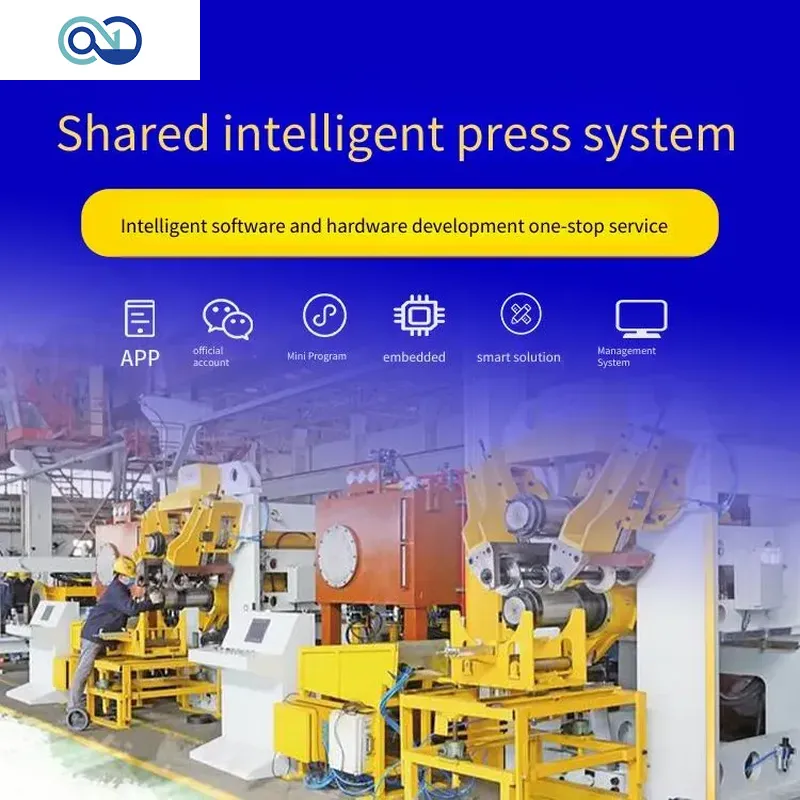
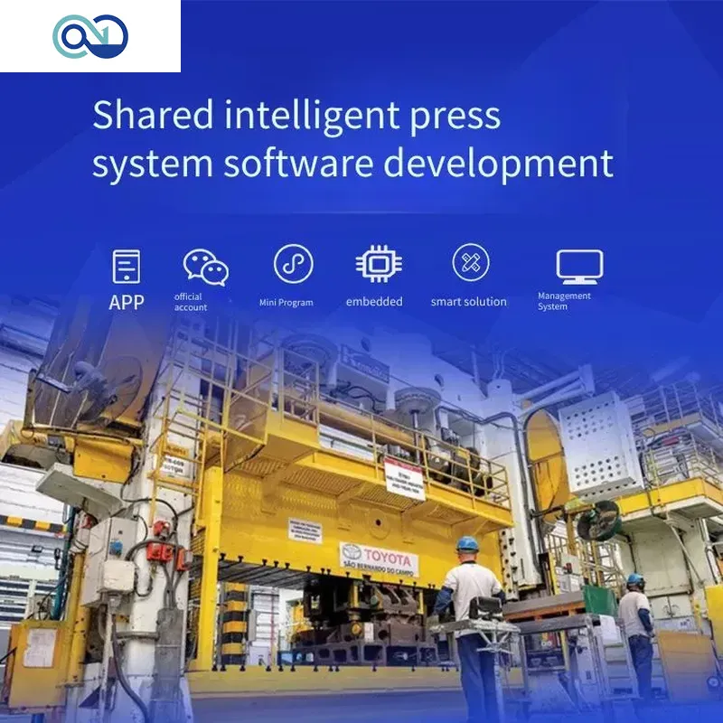
In the fast-paced world of electronics, bringing innovative products to market demands unprecedented speed and efficiency in PCB prototyping and assembly. Traditional manufacturing models often present bottlenecks, from high upfront investments in machinery to the complexities of managing diverse production volumes. Zero One Solution Limited, a leader in rapid-response R&D prototype manufacturing since 2011, introduces a game-changing approach: the Shared Smart Stamping Machine Solution. This innovative offering is designed to address the critical needs of modern product development, enabling seamless and agile production, from single prototypes to scalable batches. How can a shared smart stamping machine revolutionize your PCB assembly process and accelerate your time to market?
The Evolution of PCB Manufacturing: Why Shared Solutions?
The PCB manufacturing landscape is undergoing a significant transformation, driven by the increasing demand for faster prototyping, reduced costs, and greater flexibility. Traditional PCB assembly methods often struggle to keep pace with the rapid innovation cycles and diverse needs of modern product development. Shared smart stamping machine solutions have emerged as a compelling alternative, addressing the pain points of conventional manufacturing by offering on-demand access to advanced technology and optimized resource utilization.
What are the primary challenges of traditional PCB assembly? Traditional PCB assembly faces challenges such as high initial investment costs for equipment, long lead times for prototyping, limited flexibility in handling diverse project requirements, and the need for specialized expertise, leading to increased overheads and potential delays in product development.
Why is there a growing need for flexible PCB manufacturing models? The increasing complexity of electronic devices, coupled with shorter product lifecycles, demands more agile and flexible manufacturing processes. Flexible PCB manufacturing models enable companies to quickly adapt to changing market demands, experiment with new designs, and accelerate time-to-market without incurring prohibitive costs.
How do shared resources contribute to efficient PCB manufacturing? Shared resources, such as smart stamping machines, allow multiple companies to access state-of-the-art equipment and expertise without the burden of individual ownership. This collaborative approach optimizes resource utilization, reduces capital expenditure, and fosters innovation by providing access to advanced technologies that might otherwise be unaffordable.
What are the key benefits of adopting a shared smart stamping machine solution for PCB prototyping? Adopting a shared smart stamping machine solution offers several advantages, including reduced capital expenditure, faster turnaround times for prototypes, increased flexibility in design iterations, access to advanced stamping technology, and scalability to support both low-volume and high-volume production runs.
In what ways do shared solutions address the pain points of modern product development cycles? Shared solutions alleviate the challenges of modern product development by providing cost-effective access to cutting-edge PCB manufacturing technology, enabling rapid prototyping and design iteration, and fostering collaboration and knowledge sharing among different companies, ultimately accelerating the innovation process.
How do shared smart stamping machine solutions reduce overheads in PCB manufacturing? By eliminating the need for individual investment in expensive equipment, maintenance, and specialized personnel, shared smart stamping machine solutions significantly reduce overhead costs. Companies can access the benefits of advanced technology on a pay-per-use basis, optimizing resource allocation and improving overall cost-effectiveness.
What role does automation play in shared smart stamping machine solutions? Automation is central to shared smart stamping machine solutions, enabling precise and efficient PCB production with minimal human intervention. Automated processes ensure consistent quality, reduce the risk of errors, and accelerate production cycles, allowing companies to meet demanding timelines and achieve optimal performance.
Introducing Zero One Solution's Shared Smart Stamping Machine
At Zero One Solution Limited, we're revolutionizing PCB assembly with our state-of-the-art Shared Smart Stamping Machine. This innovative solution combines advanced technology, precision, and automation to deliver high-quality PCB assembly for a wide array of applications. It stands out in the market by offering unparalleled precision and speed, catering to both rapid prototyping and mass production needs.
What are the core features of Zero One Solution's Smart Stamping Machine? Our smart stamping machine boasts features such as high-precision stamping, automated material handling, real-time monitoring and control, and seamless integration with CAD/CAM software. It supports a wide range of materials and thicknesses, ensuring versatility for diverse PCB designs.
How does the Shared Smart Stamping Machine enhance PCB assembly quality? The machine's precision stamping process minimizes errors and ensures consistent quality across all PCBs. Advanced sensors and control systems monitor the stamping process in real-time, making immediate adjustments to maintain optimal performance.
What level of automation does the machine offer? The Shared Smart Stamping Machine features a high degree of automation, from material loading and unloading to automated tool changes and quality inspection. This reduces the need for manual intervention, minimizes human error, and speeds up the production process.
Is the Smart Stamping Machine suitable for both prototyping and mass production? Yes, our Shared Smart Stamping Machine is designed to handle both low-volume prototyping and high-volume mass production. Its flexibility and quick setup times make it ideal for rapid prototyping, while its speed and automation capabilities make it efficient for mass production runs.
What types of PCBs can be manufactured using this machine? Our machine is capable of handling a wide variety of PCB types, including single-layer, double-layer, and multi-layer PCBs. It supports different materials such as FR-4, aluminum, and flexible substrates, making it suitable for diverse applications across various industries.
How does Zero One Solution ensure the reliability and uptime of the Shared Smart Stamping Machine? We provide comprehensive maintenance and support services, including remote diagnostics, on-site repairs, and preventive maintenance programs. Our team of experienced technicians ensures that the machine operates at peak performance, minimizing downtime and maximizing productivity.
What makes Zero One Solution's Shared Smart Stamping Machine different from other solutions in the market? Our solution combines cutting-edge technology with a user-friendly design and comprehensive support services. We offer unparalleled precision, speed, and flexibility, making it the ideal choice for companies looking to streamline their PCB assembly processes and accelerate their time to market. The 'shared' aspect also allows access to advanced stamping capabilities without the full capital expenditure.
Key Benefits: Efficiency, Cost-Effectiveness, and Scalability
The shared smart stamping machine solution from Zero One Solution Limited provides significant advantages in efficiency, cost-effectiveness, and scalability for PCB manufacturing. By reducing capital expenditure and optimizing production timelines, this model offers tangible benefits for businesses of all sizes, from those engaged in low-volume R&D to high-volume production.
How does a shared smart stamping machine solution improve efficiency? A shared solution enhances efficiency by optimizing machine utilization. Instead of each company owning and maintaining its own stamping machine (which may sit idle for significant periods), multiple companies can share access to a single machine. This reduces downtime, ensures continuous operation, and maximizes throughput, which translates to faster turnaround times for PCB production.
What specific cost savings can be achieved using a shared smart stamping machine? The primary cost saving comes from reduced capital expenditure. Purchasing, maintaining, and upgrading stamping machines can be expensive. By using a shared model, businesses avoid these upfront and ongoing costs. Additional savings are realized through lower operational costs, such as reduced energy consumption, maintenance fees, and the need for specialized operators.
How does scalability work with a shared smart stamping machine solution? Scalability is a key advantage. A shared stamping machine allows businesses to easily scale their production up or down based on demand, without the constraints of fixed equipment capacity. This flexibility is particularly valuable for companies experiencing fluctuating production needs or those involved in rapid prototyping and testing.
Can small businesses benefit from a shared smart stamping machine? Absolutely. Small businesses and startups often have limited capital. A shared solution provides access to advanced stamping technology that would otherwise be unaffordable. This levels the playing field, enabling smaller companies to compete with larger ones in terms of production capabilities and product quality.
What about the quality of PCBs produced using a shared smart stamping machine? Shared smart stamping machines, like those offered by Zero One Solution Limited, are designed to maintain high levels of precision and quality. Regular maintenance, calibration, and quality control checks are integral to the shared service model. This ensures that all users receive PCBs that meet stringent quality standards.
How does using a shared smart stamping machine impact R&D and prototyping? Shared smart stamping machines significantly accelerate R&D and prototyping. The cost-effectively and quickly producing prototypes empowers engineers to test designs and iterate rapidly, reducing time-to-market for new products.
What are the long-term benefits of adopting a shared smart stamping machine solution? Long-term benefits include improved financial stability through reduced capital expenditures and operational costs, increased competitiveness due to access to advanced technology, and enhanced agility in responding to market demands. Businesses can focus on their core competencies—design and innovation—rather than being burdened by the challenges of managing and maintaining stamping equipment.
Technical Deep Dive: How Our Smart Stamping Machine Works
Our Shared Smart Stamping Machine integrates advanced technology to transform PCB design files into physical boards with unparalleled precision and efficiency. The process encompasses several key stages, each optimized for seamless operation and high-quality output, leveraging intelligent automation and rigorous quality control.
Design File Submission & Verification The process begins with the secure submission of your PCB design files (Gerber, CAD). Our system automatically verifies the files for manufacturability, identifying potential issues such as trace widths, spacing violations, and drill sizes. This automated check ensures that the design meets the required specifications before production begins, preventing costly errors and delays.
Intelligent Automation System Our smart stamping machine is equipped with an intelligent automation system that controls the entire stamping process. This system optimizes parameters such as stamping pressure, dwell time, and toolpath based on the design specifications and material properties. Real-time feedback loops continuously monitor and adjust these parameters, ensuring consistent and accurate stamping results.
Precision Stamping Process The heart of the system lies in its precision stamping process. High-accuracy stamping tools, coupled with advanced motion control, ensure that each feature is stamped with exceptional accuracy. The machine supports a wide range of materials and thicknesses, accommodating diverse PCB design requirements. The stamping process is optimized to minimize material waste and reduce production costs.
Quality Control Mechanisms Quality is paramount. Our smart stamping machine incorporates multiple quality control mechanisms throughout the process. These include automated optical inspection (AOI) systems that detect defects such as misalignments, shorts, and opens. Statistical process control (SPC) techniques are employed to monitor key process parameters and identify potential deviations from the target values. Data is collected and analyzed to continuously improve the stamping process and ensure consistent quality.
Seamless Integration with PCB Assembly The stamped PCBs are seamlessly integrated into the subsequent assembly processes. Our system ensures accurate alignment and placement of components, minimizing the risk of assembly errors. The stamped boards are compatible with standard assembly equipment, allowing for efficient and cost-effective production. This seamless integration reduces turnaround times and ensures high-quality finished products.
Final Product and Delivery The final stage involves a thorough inspection of the assembled PCBs to ensure they meet all quality requirements. Our team conducts functional testing to verify the performance of the boards. Once the boards pass all quality checks, they are carefully packaged and shipped to the customer. We offer fast and reliable delivery services to meet our customers' timelines.
Applications Across Industries: Who Benefits Most?
Our Shared Smart Stamping Machine Solution is engineered to serve a multitude of industries, providing unparalleled precision and efficiency in PCB manufacturing. From cutting-edge consumer electronics to mission-critical automotive systems, sensitive medical devices, and robust industrial controls, our solution accelerates product development cycles and streamlines production. Here’s a look at how various sectors are leveraging our innovative technology to stay ahead in today’s fast-paced market.
Consumer Electronics In the consumer electronics sector, where rapid innovation is key, our solution supports the fast prototyping and production of PCBs for smartphones, wearables, and various IoT devices. The precision and speed of our smart stamping machine enable manufacturers to quickly iterate designs and bring products to market faster, gaining a competitive edge.
Automotive The automotive industry relies on high-quality, reliable PCBs for a wide range of applications, from engine control units (ECUs) to advanced driver-assistance systems (ADAS). Our shared smart stamping machine ensures the precision and consistency required for these critical components, enhancing vehicle safety and performance.
Medical Devices For medical device manufacturers, precision and reliability are paramount. Our solution supports the production of PCBs for medical imaging equipment, patient monitoring systems, and implantable devices, adhering to stringent quality standards and regulatory requirements. The accuracy of our smart stamping machine ensures the flawless operation of these life-saving devices.
Industrial Controls In the industrial sector, our solution facilitates the production of PCBs for control systems, automation equipment, and power supplies. The robustness and efficiency of our smart stamping machine ensure the reliable operation of these critical components, even in harsh environments, minimizing downtime and maximizing productivity.
Aerospace The aerospace industry demands the highest levels of precision and reliability in PCB manufacturing. Our shared smart stamping machine solution meets these stringent requirements, supporting the production of PCBs for avionics, communication systems, and satellite technology. The accuracy and consistency of our solution ensure the safe and efficient operation of aerospace equipment.
Telecommunications The telecommunications sector relies on advanced PCBs for network infrastructure, communication devices, and data transmission equipment. Our solution enables the rapid prototyping and efficient production of these critical components, supporting the continuous expansion and improvement of communication networks. The scalability of our smart stamping machine ensures that manufacturers can meet the growing demand for high-performance telecommunications equipment.
Zero One Solution Limited: Your Partner in PCB Innovation
At Zero One Solution Limited, we understand that PCB innovation is more than just manufacturing; it's about partnership, expertise, and a relentless commitment to quality and customer success. Since our inception in 2011, we've been dedicated to providing comprehensive, one-stop services that span the entire PCB lifecycle, from initial design to final assembly. Our shared smart stamping machine solution is a testament to this commitment, embodying our dedication to empowering businesses with cutting-edge technology and unparalleled support.
As a trusted partner in the global PCBA supply chain, Zero One Solution Limited offers:
Comprehensive One-Stop Services We provide a full spectrum of services, covering everything from PCB design and rapid prototyping to manufacturing and assembly. This integrated approach streamlines the entire process, reducing complexity and accelerating time to market.
Expertise and Experience Leverage our extensive knowledge and years of experience in the PCB industry. Our team of skilled engineers and technicians are dedicated to delivering innovative solutions that meet the evolving needs of our clients.
Commitment to Quality Quality is at the heart of everything we do. We adhere to stringent quality control processes to ensure that every PCB meets the highest standards of performance and reliability.
Global PCBA Supply Chain Network With headquarters in Shenzhen, China's electronic manufacturing hub, and a branch office in Dubai, we are strategically positioned within a global supply chain network, ensuring seamless access to worldwide resources and support.
Customer-Centric Approach We prioritize our customers' needs, working closely with them to understand their unique requirements and provide tailored solutions that drive their success. Our shared smart stamping machine solution exemplifies our commitment to providing PCB solutions that empower businesses to achieve their production goals with efficiency and reliability.
By partnering with Zero One Solution Limited, you gain access to unparalleled expertise in PCB manufacturing and advanced technology that delivers superior results. Contact us today to discover how our shared smart stamping machine solution can revolutionize your PCB production process.
The Shared Smart Stamping Machine Solution from Zero One Solution Limited represents a significant leap forward in PCB assembly. By offering unparalleled flexibility, cost efficiency, and access to cutting-edge technology without the burden of ownership, we empower businesses to innovate faster and smarter. Headquartered in Shenzhen and with a branch in Dubai, our global reach ensures seamless support. Ready to transform your PCB prototyping and production? Contact Zero One Solution Limited today to discover how our shared smart stamping machine solution can accelerate your product development and deliver a competitive edge.