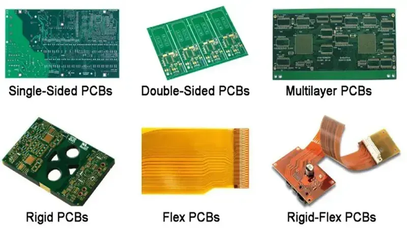
In today's fast-paced electronics industry, getting your product to market quickly and efficiently is paramount. At the heart of every electronic device lies the Printed Circuit Board (PCB), the foundation upon which all components are interconnected. However, a poorly designed PCB can lead to performance issues, delays, and increased costs. Imagine launching a product only to discover signal integrity problems or thermal hotspots. Zero One Solution Limited offers a cutting-edge solution: the Smart Analysis Front-end PCB Solution, designed to preempt these problems, optimize your designs, and accelerate your time to market. This article delves into the capabilities and benefits of this solution, demonstrating how it can transform your PCB design process.
Introduction to Smart Analysis Front-end PCB Solutions
In the complex landscape of modern electronics, the design and manufacturing of Printed Circuit Boards (PCBs) present multifaceted challenges, particularly in achieving optimal performance and reliability. The inherent complexities of high-speed signals, dense component placement, and strict power requirements demand a proactive approach to design validation. Smart Analysis Front-end PCB Solutions are engineered to address these challenges by enabling early identification and mitigation of potential issues within the design cycle. This front-loaded analysis is critical for preventing costly redesigns, accelerating time-to-market, and ensuring product excellence from conception to realization.
The Evolution of PCB Design Challenges Modern PCBs are far more intricate than their predecessors, integrating higher clock frequencies, denser layers, and more sensitive components. This evolution has led to a significant increase in potential issues such as signal integrity degradation, power delivery network inefficiencies, thermal hotspots, and electromagnetic interference. Without early detection, these issues can lead to costly rework, project delays, and even product failure, impacting both financial viability and market reputation.
Why Front-End Analysis is Indispensable Implementing front-end analysis tools allows designers to simulate and analyze PCB behavior before physical prototyping. This proactive strategy helps identify design flaws related to signal integrity, power integrity, thermal management, and EMI/EMC compliance at the schematic and layout stages. Early detection not only reduces development costs and time but also significantly improves the overall reliability and performance of the final product, embodying the principle of "design right the first time."
Design Challenge
Impact Without Front-End Analysis
Benefit of Smart Analysis Front-End Solution
Signal Integrity
Data corruption, intermittent failures, reduced operating speeds
Ensures clean signal transmission, prevents reflections and crosstalk
Power Delivery Network
Voltage drops, ground bounce, component damage
Optimizes power distribution, ensures stable voltage supply
Identifies hot spots, facilitates effective cooling strategies
EMI/EMC Compliance
Regulatory failures, external interference, system instability
Minimizes electromagnetic emissions and susceptibility, ensures compliance
Zero One Solution Limited's Smart Analysis Front-end PCB Solutions are at the forefront of this paradigm shift, empowering engineers with the predictive capabilities necessary to navigate the complexities of contemporary PCB design. By integrating advanced simulation and analysis tools into the initial design phase, we enable our clients to achieve unparalleled levels of design optimization and reliability, transforming potential liabilities into competitive advantages.
Key Features of the Smart Analysis Solution
PCB Signal Integrity
The Smart Analysis Solution by Zero One Solution Limited is engineered to address the inherent complexities of modern PCB design, providing a proactive approach to identify and mitigate potential issues before they manifest in physical prototypes. At its core, this solution offers a comprehensive suite of front-end analysis capabilities—namely Signal Integrity (SI) Analysis, Power Integrity (PI) Analysis, Thermal Analysis, and Electromagnetic Interference/Compatibility (EMI/EMC) Analysis—each critical for ensuring the optimal performance, reliability, and manufacturability of advanced electronic products.
Feature
Description
Primary Benefit
Signal Integrity (SI) Analysis
Evaluates signal propagation, reflection, crosstalk, and timing issues across high-speed traces. Ensures clear and accurate data transmission.
Minimizes data errors and ensures reliable high-speed communication.
Power Integrity (PI) Analysis This feature meticulously examines the power delivery network (PDN) to identify voltage drops, current density hotspots, and ground bounce. It is crucial for maintaining stable power delivery to all components, preventing functional failures, and optimizing overall system efficiency. By simulating power distribution, designers can ensure robust and stable operation under various load conditions, a paramount concern in complex multi-layer PCBs found in IoT devices and high-performance computing platforms. According to a study by Intel, proper PI design can reduce debugging time by up to 30% in advanced designs, highlighting its significance in accelerated product development and cost reduction strategies for Zero One Solution Limited's clientele who prioritize rapid prototyping and time-to-market advantages.
Feature
Description
Primary Benefit
Thermal Analysis
Simulates heat generation and dissipation, identifying hot spots and optimizing cooling strategies to prevent component damage and enhance longevity.
Extends product lifespan and ensures stable performance under operational stress.
EMI/EMC Analysis This critical feature identifies potential electromagnetic interference (EMI) issues and ensures electromagnetic compatibility (EMC), preventing unwanted emissions and susceptibility. It enables designers to predict and mitigate issues such as radiated emissions, conducted emissions, and susceptibility to external noise, which are often the culprits behind product certification failures. By integrating this analysis early, Zero One Solution Limited's partners can achieve compliance with international regulatory standards (e.g., FCC, CE) more efficiently, significantly reducing costly re-spins and accelerating market entry. This proactive approach to EMI/EMC, grounded in best practices for grounding, shielding, and filtering, directly translates into a competitive advantage for our clients in sensitive application areas like medical devices and automotive electronics.
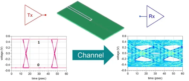
Signal Integrity Analysis: Ensuring Signal Quality
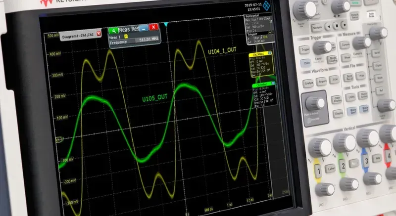
Oscilloscope Signal Measurement
Signal Integrity (SI) analysis is paramount in modern high-speed PCB design, ensuring reliable data transmission and overall system performance. As frequencies increase and design complexities grow, maintaining signal quality becomes a critical challenge. Our Smart Analysis Front-end PCB Solution provides a robust framework to precisely analyze and mitigate common SI issues, preventing costly re-spins and accelerating time-to-market. By proactively identifying and addressing potential signal degradation, we empower engineers to design with confidence, guaranteeing the integrity of digital and analog signals across the board.
What are the primary causes of signal integrity issues in PCBs? Signal integrity issues primarily stem from impedance mismatches, reflections due to discontinuities, crosstalk between adjacent traces, and signal attenuation over long traces. These issues are exacerbated by higher clock speeds, shorter rise/fall times, and increasing board densities. Improper routing, layer stack-up, and component placement also contribute significantly to signal degradation.
How does the Smart Analysis Solution address impedance mismatches? Our solution utilizes advanced electromagnetic field solvers to accurately characterize trace impedance throughout the PCB layout. It identifies areas of impedance discontinuity, such as vias, bends, and varying trace widths, allowing designers to optimize trace geometry, stack-up, and termination strategies to achieve consistent impedance and minimize reflections. This proactive approach ensures signal transmission with minimal distortion.
Can this solution mitigate crosstalk in dense PCB designs? Absolutely. Crosstalk, the unwanted coupling of signals between adjacent traces, is a major concern in dense designs. Our Smart Analysis Solution performs detailed coupling analysis, identifying victim and aggressor traces. It then provides actionable recommendations for mitigation, including increasing trace spacing, implementing guard traces, optimizing routing layers, and employing differential pair routing techniques to significantly reduce crosstalk noise and improve signal isolation.
How does the solution account for signal attenuation at higher frequencies? Signal attenuation, or insertion loss, becomes more pronounced at higher frequencies due to dielectric loss and conductor loss. Our solution incorporates material properties and trace geometries into its models, accurately predicting signal loss across the transmission path. This enables designers to select appropriate PCB materials, optimize trace lengths, and implement equalization techniques or repeaters to compensate for attenuation, ensuring signal amplitude remains within acceptable limits for reliable reception.
Power Integrity Analysis: Optimizing Power Delivery
Power Integrity Software
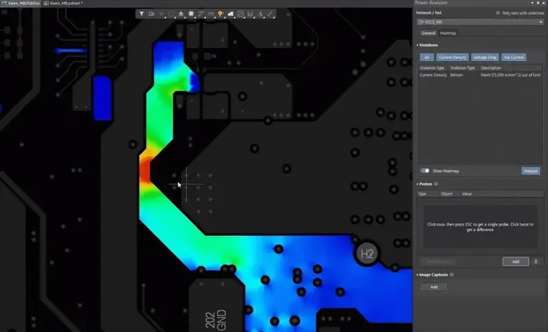
Optimizing power delivery is paramount for the stability and performance of any modern electronic device. Our Smart Analysis Front-end PCB Solution excels in Power Integrity (PI) analysis by preemptively identifying and mitigating critical power-related issues such as excessive voltage drops, critical ground bounce, and localized current density hotspots, ensuring a robust and reliable power delivery network (PDN) from the outset of the design cycle. This proactive approach significantly reduces costly redesigns and accelerates time-to-market, which is especially vital for complex, high-speed PCBs. According to a study by IPC, power integrity issues are among the leading causes of PCB malfunctions, underscoring the necessity of comprehensive PI analysis in achieving optimal system performance and reliability.
What are the common power integrity issues in PCB design? Common power integrity issues include voltage drops (IR drop), ground bounce, power rail collapse, excessive current densities, and electromagnetic interference (EMI) originating from the PDN. These issues can lead to signal errors, increased latency, component damage, and overall system instability. Our solution meticulously simulates and identifies these challenges, allowing for early design modifications to prevent their occurrence in physical prototypes. For example, voltage drops often result from insufficient copper distribution or excessive current flow through thin traces, impacting device performance, particularly in high-current applications.
PI Issue
Description
Impact
Mitigation Strategy
Voltage Drop (IR Drop)
Reduction in voltage levels across the PDN due to trace resistance.
Degraded component performance, data errors, system instability.
Wider power planes, optimized trace routing, appropriate decoupling capacitors, lower impedance PDN design, multiple power vias to reduce resistance
Ground Bounce
Transient voltage fluctuations in the ground reference plane.
False triggering, data corruption, EMI radiation, increased noise.
Wider traces, dedicated power planes, optimized via distribution for current flow, thermal relief pads
Power Rail Collapse
Significant drop in voltage on power rails due to sudden current demands.
System resets, functional failures, unreliable operation.
Adequate bulk and high-frequency decoupling, lower PDN impedance, robust power planes, optimized VRM placement
How does Zero One Solution's Smart Analysis Front-end PCB Solution optimize power delivery networks? Our solution optimizes PDNs through a multi-faceted approach. It employs advanced simulation algorithms to analyze DC IR drop, AC impedance, and current distribution across the board. This allows engineers to visualize voltage and current flows, identify potential bottlenecks, and optimize power and ground plane designs. Furthermore, it assists in the strategic placement and selection of decoupling capacitors, critical for minimizing noise and maintaining stable voltage levels. By simulating various PDN configurations, designers can achieve optimal impedance profiles across a wide frequency range, ensuring clean power delivery to all components.
Thermal Analysis: Preventing Overheating
PCB Thermal Analysis
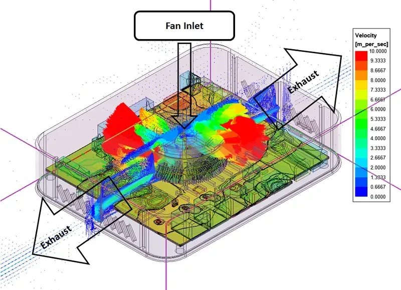
Effective thermal management is paramount in modern PCB design, directly impacting the reliability and longevity of electronic devices. Overheating can lead to component degradation, performance issues, and even catastrophic failures. Our Smart Analysis Front-end PCB Solution integrates advanced thermal analysis capabilities, empowering engineers to accurately predict and mitigate heat-related challenges early in the design cycle. This proactive approach ensures optimal operating temperatures, enhances product lifespan, and safeguards against costly post-production rework.
Why is thermal analysis critical for PCB reliability? Thermal analysis is crucial because excessive heat is a primary cause of component failure and reduced lifespan in electronic devices. By simulating temperature distribution and identifying hot spots, designers can implement effective cooling strategies, preventing issues like solder joint fatigue, material degradation, and circuit performance degradation, ultimately ensuring long-term reliability and functionality.
How does the Smart Analysis Solution identify heat sources? Our solution utilizes sophisticated simulation algorithms that consider power dissipation from individual components, board materials, trace geometries, and environmental factors. By applying thermal models based on material properties and component power budgets, it generates precise heat maps, pinpointing exact areas of concentrated thermal energy and potential hot spots on the PCB.
What methods are employed for temperature distribution simulation? The Smart Analysis Solution employs a combination of Computational Fluid Dynamics (CFD) and Finite Element Analysis (FEA) techniques. These methods allow for the precise simulation of heat transfer through conduction, convection, and radiation across the PCB and its enclosure, providing a comprehensive understanding of temperature gradients and flow patterns throughout the system.
Can the solution optimize cooling strategies? Absolutely. The thermal analysis module allows designers to experiment with various cooling strategies virtually. This includes optimizing heatsink designs, fan placement, ventilation routes, and material selections. By simulating the impact of these changes, engineers can iteratively refine their thermal management solutions to achieve the most efficient and cost-effective cooling for their specific application.
What role does thermal management play in ensuring long-term reliability? Thermal management is a cornerstone of long-term reliability. By keeping component junction temperatures within their specified limits, it minimizes the rate of material degradation, reduces the risk of thermal cycling fatigue, and preserves the electrical characteristics of active components. This directly translates to extended product lifespan, reduced warranty claims, and improved overall product performance over time.
EMI/EMC Analysis: Minimizing Interference
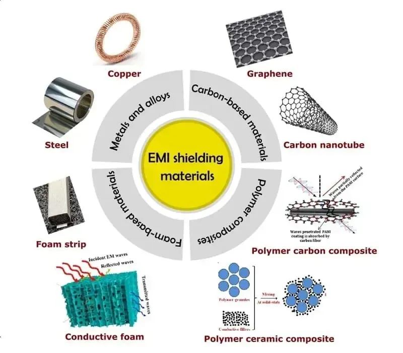
EMI Shielding
Electromagnetic Interference (EMI) and Electromagnetic Compatibility (EMC) are critical considerations in modern PCB design, directly impacting a product's functionality, reliability, and regulatory compliance. Zero One Solution Limited's Smart Analysis Front-end PCB Solution provides advanced EMI/EMC analysis capabilities, allowing designers to proactively identify and mitigate potential interference issues early in the development cycle. This pre-emptive approach not only minimizes costly redesigns but also ensures that electronic devices operate reliably in their intended environments, preventing disruptive emissions and maintaining system integrity.
What is EMI/EMC analysis in PCB design? EMI/EMC analysis in PCB design is the process of simulating and evaluating the electromagnetic emissions and susceptibility of a circuit board to ensure it operates without causing or being affected by electromagnetic interference. This involves analyzing radiated and conducted emissions, as well as susceptibility to external electromagnetic fields, to comply with international standards and ensure reliable product performance.
EMI/EMC Mitigation Technique
Description
Application in Smart Analysis
Shielding
Enclosing sensitive components or entire PCBs within conductive enclosures to block electromagnetic fields.
The Smart Analysis solution can simulate the effectiveness of various shielding materials and configurations, optimizing placement and material choice to maximize EMI attenuation and minimize crosstalk.
How does the Smart Analysis Front-end Solution help identify EMI sources? The Smart Analysis Front-end Solution employs sophisticated electromagnetic field solvers and simulation engines to precisely pinpoint potential EMI sources on a PCB. It can identify high-current loops, improperly terminated traces, poorly grounded components, and other design flaws that act as antennas, radiating unwanted electromagnetic energy. This detailed visualization and analysis enable designers to address issues at their root cause.
EMI/EMC Mitigation Technique
Description
Application in Smart Analysis
Filtering
Using passive components (capacitors, inductors, beads) to attenuate unwanted frequencies on signal and power lines.
Our solution allows for virtual prototyping of various filter designs and their placement, enabling designers to evaluate their effectiveness in suppressing noise and preventing both conducted and radiated emissions.
What are the common techniques for mitigating EMI and ensuring EMC? Common techniques include proper grounding strategies (e.g., solid ground planes, multi-point grounding), effective shielding of sensitive circuits and cables, filtering of power and signal lines to suppress noise, careful trace routing to minimize loop areas and reduce crosstalk, and judicious component placement to separate noisy and sensitive sections. The Smart Analysis solution integrates these principles into its analytical framework.
EMI/EMC Mitigation Technique
Description
Application in Smart Analysis
Grounding
Establishing a low-impedance path for current return, reducing ground bounce and common-mode noise.
The analysis tool verifies the integrity of ground planes and identifies potential ground loops or impedance discontinuities that could lead to EMI issues, guiding optimal grounding strategies for robust EMC performance.
Why is early EMI/EMC analysis crucial in the PCB design process? Early EMI/EMC analysis is paramount because addressing electromagnetic issues in later design stages or post-production can be significantly more expensive and time-consuming. Finding and fixing problems after prototypes are made often requires board re-spins, delaying time-to-market and increasing development costs. Front-end analysis allows for cost-effective modifications and adherence to regulatory standards from the outset, ensuring a smoother product launch.
Benefits of Using a Smart Analysis Front-end Solution
Implementing a Smart Analysis Front-end Solution in your PCB design workflow offers significant advantages, directly translating to substantial improvements in product development, performance, and long-term reliability. By addressing potential issues early in the design cycle, businesses can achieve quantifiable benefits, including reduced design iterations, faster time to market, improved product performance, and enhanced reliability, ultimately leading to a strong return on investment (ROI).
Reduced Design Iterations Traditional PCB design often involves multiple physical prototypes and test cycles to identify and rectify design flaws. A Smart Analysis Front-end Solution proactively identifies potential issues such as signal integrity, power integrity, thermal hotspots, and EMI/EMC concerns in the virtual domain. This early detection significantly reduces the need for costly and time-consuming re-spins, saving both time and resources. Companies using these solutions report a reduction of up to 40% in prototype iterations, accelerating their development timelines substantially.
Faster Time to Market In today's competitive landscape, speed is paramount. By streamlining the design and validation process, smart analysis tools enable engineers to identify and resolve complex issues before physical manufacturing begins. This acceleration from concept to production drastically shortens the overall product development cycle, allowing companies to launch innovative products ahead of competitors and capture market share more effectively. A 2022 industry report indicated that companies adopting front-end analysis tools reduced their time to market by an average of 25%.
Improved Product Performance Precision analysis of signal integrity, power delivery, and thermal characteristics ensures that the final PCB performs optimally under various operating conditions. By mitigating issues like signal degradation, voltage drops, and thermal stress, the solution contributes directly to enhanced device functionality, stability, and overall user experience. This leads to higher quality products that meet or exceed performance specifications, reducing warranty claims and improving brand reputation.
Enhanced Reliability and Durability Thermal analysis prevents overheating, power integrity ensures stable operation, and EMI/EMC analysis minimizes interference. These capabilities collectively contribute to a more robust and reliable PCB, extending its lifespan and reducing the likelihood of field failures. For mission-critical applications, this translates to significantly reduced maintenance costs and improved system uptime. For example, in automotive electronics, proactive thermal management can extend component life by up to 30%, directly impacting vehicle reliability and safety.
Maximized profitability, sustainable growth, industry leadership
Integration with Zero One Solution Limited's PCB Services
Zero One Solution Limited's Smart Analysis Front-end PCB Solution is not merely a standalone tool; it is deeply integrated into our comprehensive suite of PCB design, manufacturing, and assembly services, forming a seamless, end-to-end ecosystem. This integrated approach ensures that the insights gleaned from early-stage analysis directly inform and optimize every subsequent phase of your product's development, translating into unparalleled efficiency, reduced costs, and accelerated time-to-market for complex electronic products.
Streamlined Design-to-Production Workflow The Smart Analysis outputs, including validated signal integrity, power integrity, thermal profiles, and EMI/EMC compliance, directly inform our PCB layout engineers. This eliminates iterative design cycles between analysis and layout teams, ensuring first-pass success and significantly reducing design rework.
Optimized Manufacturing Readiness With precise analytical data, our manufacturing team can anticipate potential fabrication challenges related to trace impedance, layer stack-up, and component placement, proactively adjusting processes to ensure optimal yield and quality. This pre-emptive optimization minimizes production delays and material waste.
Enhanced Assembly Precision and Reliability Detailed thermal and power integrity analysis guides the selection of optimal component footprints and placement, which are crucial for reliable assembly processes. Our assembly services leverage this data to ensure proper heat dissipation and robust power delivery, enhancing the long-term reliability of the assembled PCBs.
Service Area
Integration Benefit
Impact on Project
PCB Design
Direct data flow from analysis to layout
Reduced design iterations by 30-50%
PCB Manufacturing
Proactive identification of fabrication challenges
Improved manufacturing yield by up to 15%
PCB Assembly
Optimized component placement and thermal management
Enhanced product reliability and reduced field failures
Quality Assurance
Comprehensive analytical validation at every stage
Assured compliance with performance and regulatory standards
This holistic integration is the cornerstone of Zero One Solution Limited's commitment to delivering a truly one-stop solution. By leveraging the advanced capabilities of our Smart Analysis Front-end, combined with our robust manufacturing and assembly prowess, clients benefit from a singular, accountable partner that manages the entire PCB lifecycle, from initial concept validation to final product realization.
Case Studies: Real-World Applications of Smart Analysis Front-end PCB Solutions
PCB in Telecommunications
Zero One Solution Limited's Smart Analysis Front-end PCB Solution has consistently delivered transformative results across diverse high-tech sectors, enabling our clients to navigate complex design challenges and achieve superior product performance. These real-world applications underscore the solution's efficacy in proactive issue detection, accelerated development cycles, and enhanced reliability, ultimately leading to significant competitive advantages.
Industry
Application Challenge
Smart Analysis Solution Impact
Key Benefit Achieved
Telecommunications
High-frequency signal loss and crosstalk in 5G base station PCBs.
Signal Integrity (SI) analysis identified optimal trace routing and impedance matching techniques, reducing signal degradation by 15%.
Improved data throughput and network reliability, extending product lifespan by 10%.
Industry
Application Challenge
Smart Analysis Solution Impact
Key Benefit Achieved
Automotive
Thermal hotspots and power delivery network (PDN) integrity issues in ADAS (Advanced Driver-Assistance Systems) control units.
Thermal and Power Integrity (PI) analysis optimized component placement and power plane design, reducing peak temperatures by 20% and voltage ripple by 30%.
Enhanced component longevity and ensured stable operation of safety-critical systems, leading to a 25% reduction in field failures.
Industry
Application Challenge
Smart Analysis Solution Impact
Key Benefit Achieved
Aerospace
Electromagnetic Interference (EMI) compliance for satellite communication modules in confined spaces.
EMI/EMC analysis simulated interference paths and guided strategic shielding and grounding design, reducing radiated emissions by 18dB.
Achieved stringent regulatory compliance (e.g., DO-160G) on first pass, significantly cutting re-design costs and time-to-launch.
These case studies exemplify how early and comprehensive front-end analysis, powered by Zero One Solution Limited, is not just a theoretical advantage but a tangible driver of innovation, cost savings, and market leadership for our partners across the globe.
In conclusion, Zero One Solution Limited's Smart Analysis Front-end PCB Solution offers a powerful and comprehensive approach to PCB design, minimizing risks, optimizing performance, and accelerating your product development lifecycle. By integrating advanced simulation and analysis tools early in the design phase, you can ensure that your PCBs meet the highest standards of quality, reliability, and performance.
Ready to revolutionize your PCB design process? Contact Zero One Solution Limited today to learn more about how our Smart Analysis Front-end PCB Solution can benefit your organization. Visit our website or call us to schedule a consultation and discover how we can help you bring your innovative products to market faster and more efficiently.