In the fast-paced world of gaming, the gamepad is more than just a controller; it's the player's direct interface with the virtual world. At the heart of every high-performance gamepad lies its Printed Circuit Board (PCB), the unsung hero responsible for translating your every command with precision and speed. But what does it take to create a truly 'smart' gamepad PCB? This article delves deep into the world of Smart Gamepad PCB solutions, exploring the critical design considerations, manufacturing processes, and assembly techniques that elevate a simple controller into a seamless gaming experience. Zero One Solution Limited, a leader in rapid PCB prototyping and assembly, is here to guide you through the intricacies of crafting a gamepad PCB that not only meets but exceeds the demands of modern gaming.
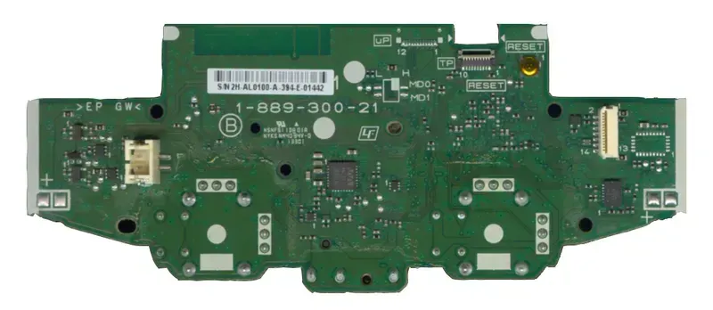
At the heart of every responsive and immersive gaming experience lies a meticulously engineered Smart Gamepad PCB. This central nervous system of the controller orchestrates precise input registration, haptic feedback, and wireless communication, transforming player commands into in-game actions. Its design directly impacts latency, durability, and overall user satisfaction, making it a critical component that demands expert consideration from concept to production. For serious gamers and developers alike, understanding the intricate architecture of a Smart Gamepad PCB is paramount to achieving unparalleled control and performance.
| Component Type | Function | Impact on Gamepad Performance |
|---|---|---|
| Input Interface (Buttons, Joysticks, Triggers) | Translates physical actions into electrical signals. | Directly affects responsiveness, precision, and tactile feedback. High-quality switches and potentiometers reduce input lag and improve durability, crucial for competitive play where milliseconds matter. Studies show that a 10ms reduction in input latency can significantly improve player reaction times in fast-paced games. |
| Component Type | Function | Impact on Gamepad Performance |
|---|---|---|
| Power Management Unit (PMU) | Regulates power supply from the battery to all components. | Ensures stable voltage, optimizes battery life, and prevents power-related issues. Efficient PMUs are vital for extended gaming sessions, with advanced designs capable of dynamic voltage scaling based on component load. |
| Component Type | Function | Impact on Gamepad Performance |
|---|---|---|
| Sensor Array (Accelerometer, Gyroscope) | Detects gamepad movement and orientation for motion control. | Expands gameplay possibilities beyond traditional button inputs, enabling intuitive aiming or steering. High-resolution sensors provide accurate and fluid motion tracking, essential for games utilizing motion controls. Many modern gamepads integrate 6-axis IMUs (Inertial Measurement Units) to capture both translational and rotational movements with high fidelity. |
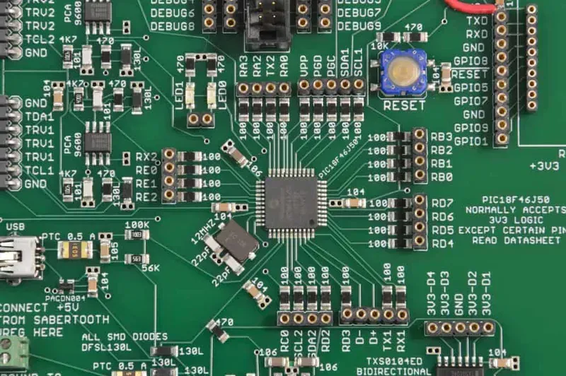
Designing a Smart Gamepad PCB for optimal performance demands meticulous attention to critical aspects beyond mere component selection. The interplay of component placement, signal integrity, and power management is paramount in achieving a responsive, reliable, and high-performance gaming peripheral. Overlooking these fundamental design principles can lead to latency, signal degradation, and diminished user experience, ultimately hindering the gamepad's competitive edge.
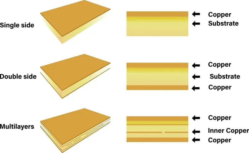
Selecting the appropriate PCB materials is fundamental to the performance and durability of a Smart Gamepad. Given the demanding nature of gaming applications, where precise signal transmission, robust mechanical integrity, and effective thermal management are paramount, the choice of substrate significantly impacts the final product's reliability and user experience. The right foundation ensures that the gamepad can withstand repeated use, maintain signal integrity for responsive control, and dissipate heat efficiently to prevent component degradation. For Smart Gamepad PCB Solutions, this means considering factors beyond basic electrical properties, delving into aspects like dielectric constant stability, excellent mechanical strength, and thermal conductivity to ensure optimal functionality under various operating conditions.
| Material Type | Key Advantage for Gamepads | Consideration |
|---|---|---|
| FR-4 | Cost-effective, good general performance, widely available | Dielectric constant variations with frequency, moderate thermal conductivity |
| High-Tg FR-4 | Improved thermal resistance, increased durability under heat | Slightly higher cost than standard FR-4 |
| Polyimide | Excellent thermal stability, superior mechanical strength, ideal for flexible PCBs | Higher cost, less common for rigid gamepad PCBs |
| Rogers / PTFE | Low dielectric loss, stable dielectric constant, excellent for high-frequency signals | Significantly higher cost, specialized manufacturing requirements, less mechanical rigidity |
The choice of material also extends to the copper foil and solder mask. High-quality copper foil ensures optimal current carrying capacity and signal integrity, while a durable solder mask protects against environmental factors and short circuits. For Zero One Solution Limited, our expertise lies in guiding clients through this critical material selection process, leveraging our deep understanding of the global PCBA supply chain to source materials that meet the stringent performance demands of Smart Gamepad PCB Solutions, balancing innovation with cost-efficiency.
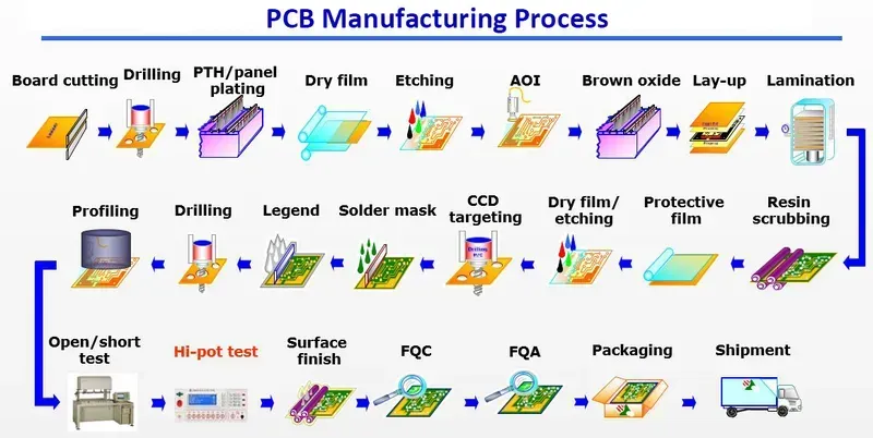
The manufacturing process of a Smart Gamepad PCB is a complex, multi-stage operation demanding unparalleled precision and stringent quality control. From initial data preparation to final inspection, each step is critical to producing a high-performance, durable, and reliable circuit board capable of withstanding the rigors of competitive gaming. Achieving this involves advanced machinery, skilled technicians, and an unwavering commitment to industry best practices, ensuring every board meets the exacting standards required for seamless gameplay.
| Manufacturing Stage | Key Process | Quality Control Focus |
|---|---|---|
| Drilling | Creating holes for vias and components using CNC drills. | Hole diameter, positional accuracy, burr minimization, clean drilling for reliable plating. |
| Plating & Electroless Copper Deposition | Depositing a thin layer of copper into drilled holes and on surfaces. | Uniformity of copper thickness, adhesion to laminate, complete coverage for conductivity. |
| Manufacturing Stage | Key Process | Quality Control Focus |
|---|---|---|
| Solder Mask Application | Applying a protective epoxy layer over copper traces, leaving pads exposed. | Uniform thickness, complete coverage over traces, precise registration to pads, prevention of solder bridges and shorts during assembly. |
Zero One Solution Limited leverages state-of-the-art manufacturing facilities and rigorous quality control protocols throughout every stage of Gamepad PCB production. Our expertise ensures that each PCB is fabricated with the utmost precision, leading to superior performance and durability, which are critical for the demanding environment of modern gaming.
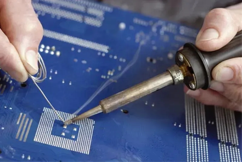
The assembly phase of a Smart Gamepad PCB is paramount, transforming a bare board into a functional, robust device. Precision in this stage directly impacts the reliability and longevity of the gamepad, ensuring consistent performance under intense gaming conditions. Effective assembly techniques, particularly advanced soldering and meticulous component mounting, are critical for minimizing defects and maximizing the operational lifespan of the PCB.
| Assembly Process | Description | Impact on Gamepad PCB |
|---|---|---|
| Solder Paste Application | Precision stencil printing of solder paste onto pads. | Ensures proper electrical connection and mechanical bond for SMDs, critical for small, intricate gamepad components like microcontrollers and sensors, preventing shorts or open circuits for consistent performance, impacting reliability directly through connection integrity and power distribution efficiency across the board. Proper application minimizes rework and enhances overall yield. |
| Pick-and-Place Machine Operation | Automated placement of SMDs onto solder paste-covered pads. | Accurate and high-speed component placement, vital for compact gamepad layouts. Incorrect placement can lead to short circuits or poor connections, resulting in intermittent functionality or complete failure. Efficiency in this step is crucial for rapid production and maintaining product quality across large batches. |
| Reflow Soldering | Heating the PCB to melt solder paste, creating permanent solder joints. | Forms reliable electrical and mechanical bonds for SMDs. Incorrect temperature profiles can cause solder defects (e.g., cold joints, voids), leading to signal loss, component damage, or premature failure. Optimal reflow ensures robust connections for all digital and analog signals, maintaining high performance under operational stress. |
| Inspection (AOI/X-Ray) | Automated Optical Inspection (AOI) and X-ray inspection to detect defects. | Crucial for identifying soldering errors, missing components, or misalignments that are undetectable by visual inspection. Ensures the integrity of all connections, particularly critical for multi-layer PCBs and fine-pitch components common in smart gamepads. Early detection prevents costly reworks and guarantees product reliability before functional testing. |
| Final Assembly & Enclosure | Mounting the assembled PCB into the gamepad casing and connecting peripherals. | Ensures the PCB is securely housed, protecting it from physical damage and environmental factors. Proper internal cabling and connector mating are essential for all buttons, joysticks, and vibration motors to function correctly. This stage is vital for the ergonomic and aesthetic aspects of the final product, directly impacting user comfort and perceived quality. |
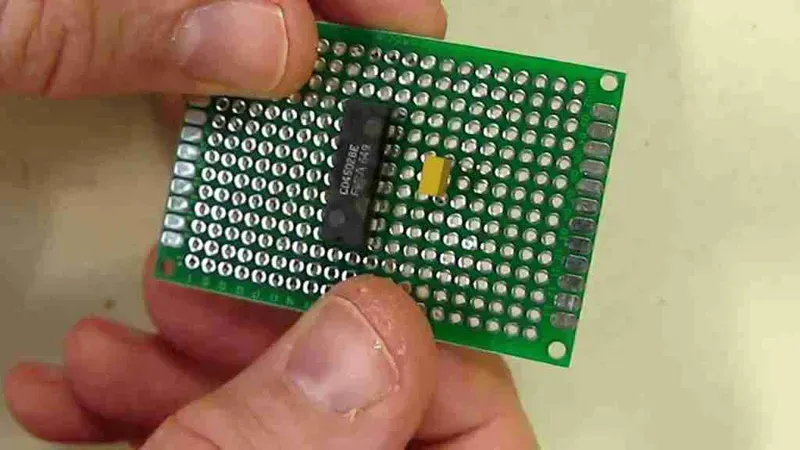
Rapid prototyping for Smart Gamepad PCBs is a cornerstone for accelerated product development, enabling manufacturers to quickly test, validate, and iterate on designs. This agile approach significantly reduces time-to-market and optimizes costs by identifying and resolving design flaws early in the development cycle, a critical advantage in the fast-paced gaming peripheral industry. By transforming theoretical designs into tangible prototypes with speed and precision, companies can gather crucial feedback and make informed decisions, ensuring the final product meets the high performance and reliability standards demanded by gamers.
Ensuring the unwavering performance and reliability of Smart Gamepad PCBs is paramount for delivering an exceptional user experience and preventing costly post-launch issues. At Zero One Solution Limited, our comprehensive testing and validation protocols are meticulously designed to scrutinize every aspect of the PCB, from individual component functionality to full system integration, guaranteeing that each board meets the rigorous demands of the gaming industry and beyond. This meticulous approach minimizes defects, optimizes operational lifespan, and ultimately safeguards brand reputation.
| Testing Phase | Key Objectives | Techniques Utilized | Benefits |
|---|---|---|---|
| In-Circuit Test (ICT) | Verify component presence, orientation, and solder joint integrity. | Bed-of-nails fixture, digital and analog measurements, open/short detection. | Early detection of manufacturing defects, reduced repair costs, high fault coverage for passive components and short circuits. |
Following ICT, functional testing takes center stage. This phase simulates real-world operating conditions, subjecting the Smart Gamepad PCB to various scenarios to confirm its operational readiness and responsiveness. This includes assessing button presses, joystick movements, haptic feedback, wireless connectivity, and power consumption under load. Our advanced functional test jigs replicate user interactions and environmental stresses, providing invaluable data on performance stability and identifying any latent defects that might not be caught by static tests. This ensures that every Smart Gamepad PCB leaving our facility is not just functional, but performs flawlessly, delivering the responsiveness and durability gamers expect.
| Testing Phase | Key Objectives | Techniques Utilized | Benefits |
|---|---|---|---|
| Functional Test (FCT) | Validate overall PCB functionality under operational conditions. | Automated test equipment (ATE), custom test fixtures, software-driven simulations of user input and outputs. | Confirms system-level performance, identifies interaction issues between components, verifies real-world responsiveness and reliability. |
Beyond standard functional testing, environmental stress testing (EST) is employed to assess the Smart Gamepad PCB's resilience against varying environmental conditions such as temperature fluctuations and humidity. This proactive approach helps predict long-term reliability and uncovers potential weaknesses that could lead to failures in diverse operating environments. Our commitment to extensive testing, leveraging techniques from ICT to EST, ensures that every Smart Gamepad PCB we produce not only meets but exceeds industry benchmarks for quality, performance, and reliability.
| Testing Phase | Key Objectives | Techniques Utilized | Benefits |
|---|---|---|---|
| Environmental Stress Test (EST) | Assess PCB durability and performance under extreme environmental conditions. | Thermal cycling, humidity testing, vibration testing. | Identifies material weaknesses, predicts long-term reliability, ensures performance stability across diverse operating environments. |
Zero One Solution Limited stands as a premier PCB solution provider, uniquely positioned to empower innovation in the gaming industry with our specialized expertise in Smart Gamepad PCBs. Our integrated approach, spanning from intricate PCB design to precision manufacturing and assembly, ensures that your gamepad concepts transcend initial ideas to become high-performance, market-ready products. We understand the critical interplay of responsiveness, durability, and ergonomic design demanded by modern gaming, and our solutions are meticulously engineered to meet and exceed these stringent requirements.
| Capability | Benefit for Smart Gamepad PCBs | Zero One Solution Advantage |
|---|---|---|
| Rapid Prototyping | Accelerated development cycles, quick design iteration | Fastest turnaround times in the industry, enabling agile product refinement |
| Advanced Material Selection | Enhanced durability, optimal signal integrity for precise control | Access to a global network of material suppliers, ensuring ideal performance-to-cost ratio |
| Precision Assembly | Reliable connections, extended product lifespan | Automated SMT lines and rigorous IPC standards for flawless component placement and soldering |
| Comprehensive Testing & Validation | Guaranteed performance, reduced field failures | Multi-stage testing protocols including functional, environmental, and stress testing tailored for gaming peripherals |
Headquartered in Shenzhen, the heart of global electronics manufacturing, with a strategic branch office in Dubai, Zero One Solution Limited is adeptly integrated into the global PCBA supply chain. This strategic footprint allows us unparalleled access to advanced technologies and high-quality components, enabling us to deliver cost-effective and cutting-edge Smart Gamepad PCB solutions. Our commitment to excellence, rapid response R&D prototyping, and unwavering focus on client success make us the ideal partner to bring your next-generation smart gamepad to life, ensuring it stands out in a competitive market.
Understanding the intricacies of Smart Gamepad PCBs is crucial for optimal performance and user experience. This section addresses frequently asked questions, providing clear and concise answers to common queries regarding their design, manufacturing, and assembly, ensuring a comprehensive grasp of these critical components.
In conclusion, a Smart Gamepad PCB solution is more than just a circuit board; it's the foundation of a superior gaming experience. From optimized design and component selection to efficient manufacturing and rigorous testing, every step is crucial in creating a reliable and high-performance controller. At Zero One Solution Limited, we're dedicated to providing comprehensive PCB solutions that empower our clients to innovate and excel in the competitive gaming market. Ready to level up your gamepad design? Contact us today to explore how our rapid prototyping and assembly services can bring your vision to life. Share your thoughts and experiences in the comments below – let's shape the future of gaming together!

