The evolution of smart grids is revolutionizing energy distribution, demanding robust and reliable communication infrastructure. At the core of this transformation are advanced Printed Circuit Boards (PCBs) that enable seamless data flow and control. As a veteran engineer at Zero One Solution Limited, I've witnessed firsthand the critical role PCBs play in this paradigm shift. Since 2011, Zero One Solution has been at the forefront, providing rapid-response R&D prototype manufacturing and comprehensive PCB solutions, empowering clients to accelerate product development. This article will delve into how our specialized Smart Grid Communication PCB Solutions are engineered to meet the stringent demands of this vital sector, ensuring efficiency, reliability, and innovation.
The smart grid represents a fundamental transformation of traditional electrical grids, integrating advanced digital communication technologies to enable real-time monitoring, control, and optimization of energy distribution. At the heart of this evolution lies the critical role of robust and reliable Printed Circuit Boards (PCBs). These components are not merely circuit carriers; they are the central nervous system, ensuring seamless data flow for everything from smart meters and renewable energy integration to demand-side management and fault detection. The operational efficiency, stability, and resilience of modern energy grids are inextricably linked to the performance and unwavering reliability of the PCBs embedded within their communication infrastructure. Without highly dependable PCBs, the promise of a truly intelligent and adaptive energy network remains unfulfilled, leading to potential outages, data integrity issues, and inefficient resource allocation. Consequently, understanding the imperative for superior PCB solutions is paramount for any stakeholder committed to advancing smart grid technologies.
| Key Smart Grid Application | Communication Imperative | PCB Role |
|---|---|---|
| Smart Meters | Accurate, real-time consumption data | Data processing, secure wireless/PLC modules |
| Distribution Automation | Reliable remote control & monitoring | High-reliability control circuits, environmental robustness |
| Renewable Energy Integration | Seamless data flow for grid synchronization | Power conversion & management, stable communication interfaces |
| Electric Vehicle Charging Infrastructure | Fast, secure transaction & load balancing | High current handling, robust data links |
| Substation Automation | High-speed, low-latency data exchange | EMI shielded, high-density digital and analog circuits |
Designing Printed Circuit Boards (PCBs) for smart grid communication systems presents a unique set of formidable challenges that demand exceptional engineering precision and material science expertise. Unlike general-purpose electronics, smart grid PCBs operate in harsh, dynamic environments, requiring extreme high reliability, impeccable data integrity, and robust environmental resilience to ensure the seamless and secure flow of energy. These stringent requirements are critical for maintaining the stability, efficiency, and security of modern energy infrastructures, directly impacting national energy security and public safety.
| Challenge | Impact on PCB Design | Zero One Solution's Approach |
|---|---|---|
| Extreme Temperatures | Thermal management, material selection for coefficient of thermal expansion (CTE) matching, delamination prevention. | Utilizing high-Tg laminates and advanced thermal vias for efficient heat dissipation and stability across wide temperature ranges (-40 y0C to +125 y0C). |
| High Humidity/Corrosion | Moisture ingress, short circuits, material degradation. | Applying specialized conformal coatings, selecting low moisture absorption materials (e.g., polyimide), and robust surface finishes (ENIG, Immersion Silver) for enhanced corrosion resistance and long-term reliability in humid environments and outdoor deployments and harsh conditions like coastal or industrial areas reducing component failure rates and ensuring signal integrity.. |
| Electromagnetic Interference (EMI) | Signal degradation, data corruption, system instability. | Implementing advanced shielding techniques, optimized ground planes, differential pair routing, and careful component placement to minimize EMI effects and ensure signal integrity, leveraging our extensive experience in high-speed and RF designs to mitigate crosstalk and external interference effectively maintaining data accuracy and system stability. |
Zero One Solution Limited stands at the forefront of providing specialized PCB solutions for the evolving smart grid landscape. Our expertise spans the entire product lifecycle, from initial design and engineering to rapid prototyping and precise assembly, all meticulously tailored to meet the stringent demands of smart grid applications. We understand that reliable communication is the backbone of smart grid efficiency and resilience, and our deep technical knowledge ensures that the PCBs we produce are not just components, but critical enablers of advanced energy management systems. Our commitment to innovation and quality positions us as a trusted partner in accelerating the deployment of next-generation smart grid technologies.

Zero One Solution's Smart Grid Communication PCBs are engineered with precision to meet the stringent demands of modern energy infrastructure. Our designs prioritize critical performance attributes, ensuring the seamless and reliable operation essential for smart grid communication networks. We focus on delivering unparalleled signal integrity, optimized power efficiency, and exceptional durability through the strategic selection of advanced materials and meticulous manufacturing processes.
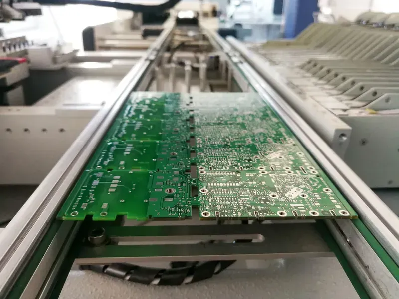
Zero One Solution Limited offers a truly comprehensive one-stop service for Smart Grid Communication PCB Solutions, providing an integrated approach that spans the entire product lifecycle from initial concept to efficient mass production. This holistic model streamlines development, mitigates risks, and ensures seamless transition between stages, ultimately accelerating your time-to-market for critical smart grid components and systems.
| Service Phase | Description | Key Benefits for Smart Grid PCBs |
|---|---|---|
| Concept & Design Validation | Collaborative engagement with client engineers to refine design specifications, select optimal materials, and perform DFM/DFA (Design for Manufacturability/Assembly) analyses. | Ensures design integrity, reduces costly redesigns, and optimizes performance for demanding smart grid environments before production begins. Identifies potential issues early, improving reliability and preventing field failures. |
| Service Phase | Description | Key Benefits for Smart Grid PCBs |
|---|---|---|
| Rapid Prototyping | Expedited fabrication of initial PCB prototypes and assembly for functional testing and iteration. Utilizes advanced manufacturing techniques to reduce lead times significantly. | Allows for quick validation of design concepts, rapid iteration on performance improvements, and faster product development cycles, crucial for agile smart grid innovation. |
| Service Phase | Description | Key Benefits for Smart Grid PCBs |
|---|---|---|
| Component Sourcing & Procurement | Leveraging a global network to source high-quality, reliable electronic components, with a focus on supply chain resilience and genuine part verification. | Guarantees access to specialized components, mitigates supply chain disruptions, and ensures the authenticity and quality of every part, vital for long-term smart grid system stability. |
| Service Phase | Description | Key Benefits for Smart Grid PCBs |
|---|---|---|
| Advanced Manufacturing & Assembly | State-of-the-art SMT (Surface Mount Technology) and THT (Through-Hole Technology) assembly lines, precise soldering, and conformal coating for environmental protection. | Achieves high-density, high-reliability assemblies compliant with IPC standards, ensuring robust performance under harsh conditions common in smart grid infrastructure. |
| Service Phase | Description | Key Benefits for Smart Grid PCBs |
|---|---|---|
| Rigorous Testing & Quality Assurance | Comprehensive testing protocols including AOI (Automated Optical Inspection), X-ray inspection, ICT (In-Circuit Test), functional testing, and environmental stress screening. | Verifies functionality, identifies defects, and ensures the highest levels of quality and reliability, minimizing field failures and supporting critical smart grid operations. |
| Service Phase | Description | Key Benefits for Smart Grid PCBs |
|---|---|---|
| Logistics & After-Sales Support | Efficient global logistics for timely delivery and dedicated after-sales support for ongoing inquiries and technical assistance. | Ensures seamless delivery of finished products worldwide and provides continuous support, reinforcing long-term partnership in the evolving smart grid landscape. |
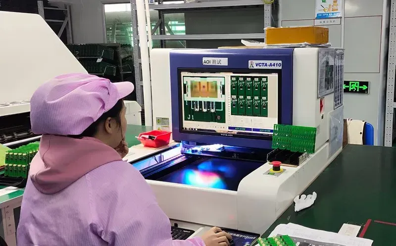
In the demanding environment of smart grid infrastructure, the integrity and uninterrupted operation of communication systems are paramount. At Zero One Solution Limited, our commitment to quality assurance and reliability in Smart Grid Communication PCB Solutions is unwavering. We understand that even a minor component failure can lead to significant disruptions, economic losses, and even safety hazards. Therefore, our processes are meticulously designed to exceed industry benchmarks, ensuring that every PCB we produce delivers uncompromising performance and durability under the most challenging conditions. This dedication is fundamental to building a resilient and efficient smart grid.
| Testing Protocol | Description | Standard Adherence | Benefit for Smart Grid |
|---|---|---|---|
| Automated Optical Inspection (AOI) | High-speed, high-resolution inspection of PCB layers and components for defects. | IPC-A-610 Class 3 | Detects subtle defects early, preventing field failures and ensuring signal integrity crucial for grid stability. |
| In-Circuit Test (ICT) | Verifies the functionality of individual components and their interconnections on the assembled PCB. | IEEE 1149.1 (JTAG) | Identifies assembly errors and component defects, guaranteeing accurate data transmission and control within the smart grid. |
| Functional Test (FCT) | Simulates the PCB's actual operational environment to validate its performance and communication capabilities. | IEC 61850 | Confirms end-to-end reliability and interoperability, ensuring seamless integration into complex smart grid networks. |
| Environmental Stress Screening (ESS) | Subjects PCBs to extreme temperature cycling, humidity, and vibration to identify latent defects. | MIL-STD-810G | Enhances long-term reliability by weeding out weak components, critical for devices deployed in diverse smart grid environments. |
| Material Traceability & Certification | Comprehensive tracking of all raw materials, components, and manufacturing processes. | ISO 9001:2015, RoHS, UL | Ensures material quality, compliance with regulations, and provides a robust audit trail, vital for critical infrastructure components. |
Our rigorous testing regimen, combined with a steadfast adherence to international industry standards, forms the bedrock of our reliability promise. Each stage of the PCB manufacturing process, from design validation to final assembly and testing, is subjected to stringent quality checks. This multi-layered approach ensures that our Smart Grid Communication PCBs are not just functional, but are built to endure, providing the robustness and longevity required for mission-critical smart grid applications.
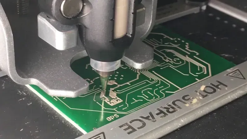
In the fast-evolving landscape of smart grid technology, speed to market is a critical competitive advantage. Zero One Solution Limited's rapid prototyping capabilities are specifically designed to accelerate the development cycle of Smart Grid Communication PCB Solutions, enabling our clients to innovate faster and deploy cutting-edge technologies with unprecedented efficiency. This swift iterative process is not just about speed; it's about fostering agile development, reducing risk, and ensuring that your smart grid innovations are robust and market-ready.

Zero One Solution Limited's strategic global presence, anchored by our headquarters in Shenzhen, China, and a branch office in Dubai, UAE, is a cornerstone of our ability to deliver superior Smart Grid Communication PCB Solutions. This dual-hub model provides unparalleled advantages in supply chain resilience, rapid logistics, and localized support, ensuring that our clients benefit from the most efficient and responsive service in the industry, regardless of their geographical location. It is this strategic positioning that allows us to seamlessly navigate the complexities of global manufacturing and distribution, ultimately accelerating time-to-market for our smart grid partners.
| Aspect | Shenzhen Headquarters Advantage | Dubai Branch Advantage | Combined Global Impact |
|---|---|---|---|
| Manufacturing & Innovation | Proximity to the world's leading electronic component suppliers and advanced manufacturing ecosystems; rapid prototyping and mass production capabilities. | Gateway to emerging markets and a hub for innovation in the Middle East and Africa. | Optimized production cycles and access to cutting-edge technologies globally. |
| Supply Chain Efficiency | Direct access to a vast network of raw material providers and specialized fabrication services, ensuring competitive pricing and swift lead times. | Strategic logistics hub for global distribution, reducing shipping times and costs to key markets. | Seamless end-to-end supply chain management, minimizing delays and maximizing cost-effectiveness. |
| Market Access & Support | Deep understanding of high-volume production demands and R&D support for complex projects. | Facilitates direct engagement with clients in diverse regions, offering localized sales and technical support. | Expansive market reach with tailored support, fostering stronger client relationships and quicker problem resolution. |
| Risk Mitigation | Diversification of manufacturing capabilities and supply routes. | Alternative logistics channels and market access points. | Enhanced supply chain resilience against geopolitical or logistical disruptions, ensuring business continuity. |
Navigating the complexities of Smart Grid Communication PCB Solutions can raise numerous questions regarding their design, manufacturing, and long-term reliability. At Zero One Solution Limited, we are committed to providing clarity and comprehensive support. This FAQ section addresses common inquiries, offering concise and authoritative answers to help you understand the critical aspects of PCBs in smart grid applications and how our expertise ensures optimal performance and efficiency for your projects.
In conclusion, the future of smart grids hinges on advanced, reliable communication, underpinned by sophisticated PCB technology. Zero One Solution Limited, with over a decade of expertise in rapid prototyping and comprehensive PCB solutions, is uniquely positioned to be your strategic partner. Our commitment to quality, efficiency, and innovation ensures that your smart grid communication infrastructure is built on the most robust foundation. From our Shenzhen headquarters to our Dubai branch, we are dedicated to empowering your success. We invite you to connect with Zero One Solution Limited to explore how our Smart Grid Communication PCB Solutions can accelerate your next project and contribute to a more connected, efficient energy future. Experience the difference of partnering with a leader in PCB assembly solutions – contact us today to discuss your specific requirements.

